Memory Basis
约 1520 个字 20 张图片 预计阅读时间 5 分钟
Abstract
-
存储器基本概念
Basic concepts of memory- 存储器定义、RAM 的定义、存储器地址概念定义、存储器基本数据单元和操作
Memory definitions, RAM, memory address, RAM cell, basic memory operations
- 存储器定义、RAM 的定义、存储器地址概念定义、存储器基本数据单元和操作
-
存储器的组织
memory organization- 地址、字长和存储单元个数之间关系
Relationship between address, word width and storage cells
- 地址、字长和存储单元个数之间关系
-
存储器的基本结构框图
Memory block diagram- 地址线、数据线、控制线
Address lines, Data lines, Control lines
- 地址线、数据线、控制线
-
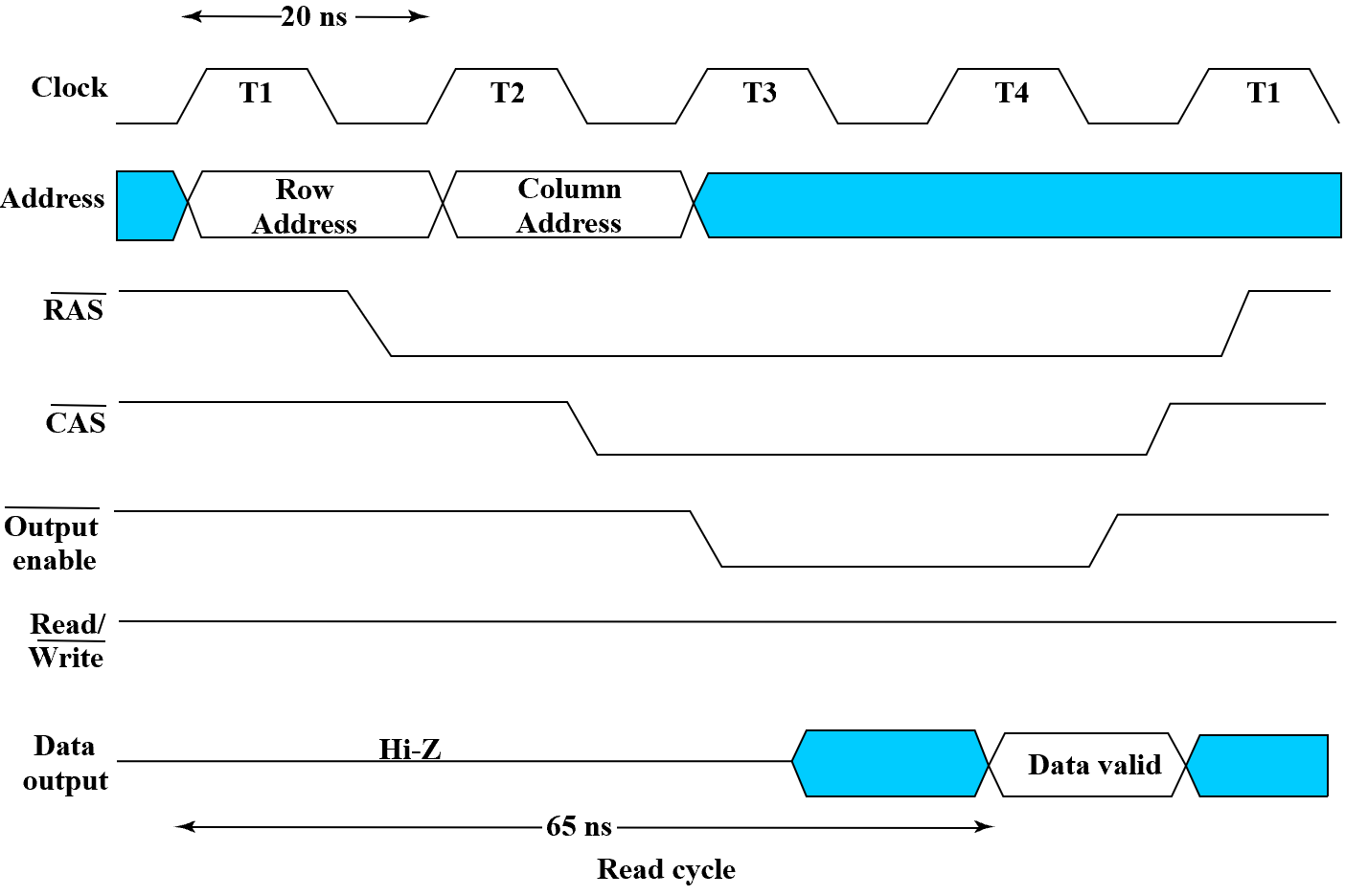
读、写过程中各信号的时序、DRAM 的访问时序
Memory Read or Write Operation Timing, DRAM Read Timing -
静态 RAM 和动态 RAM 的基本概念
Basic concepts of Static RAM and Dynamic RAM- 静态存储器 SRAM 结构、动态存储器 DRAM 结构、区别
Structure and difference of SRAM and DRAM
- 静态存储器 SRAM 结构、动态存储器 DRAM 结构、区别
-
DRAM 控制电路与刷新
DRAM block diagram and refresh - 两次(分时)地址加载,先加载行地址后加载列地址
Row Address and Column Address - 存储器的字扩展和位扩展方法
Memory word expansion and width expansion - 同步 SDRAM 的猝发读的基本概念
Burst read in SDRAM
Memory Concepts
- Memory ─ A collection of storage cells together with the necessary circuits to transfer information to and from them.
一组存储单元的集合,可以读、写。 - Memory Organization ─ the basic architectural structure of a memory in terms of how data is accessed.
内存的架构,内存能存放多少数据,一个字多少位,如何访问内存等。 - Random Access Memory (RAM) ─ a memory organized such that data can be transferred to or from any cell (or collection of cells) in a time that is not dependent upon the particular cell selected.
- Memory Address ─ A vector of bits that identifies a particular memory element (or collection of elements).
内存地址,一个列表的编号,通过编号可以读写内存的数据。
Typical data elements are:
- bit
- byte ─ 8 bits
-
word ─ a collection of binary bits whose size is a typical unit of access for the memory. It is typically a power of two multiple of bytes (e.g. 1 byte, 2 bytes, 4 bytes, 8 bytes, etc. )
不同计算机的字长可能不同。 -
Memory Data ─ a bit or a collection of bits to be stored into or accessed from memory cells.
- Memory Operations ─ operations on memory data supported by the memory unit. Typically, read and write operations over some data element (bit, byte, word, etc ).
Memory Organization
Organized as an indexed array of words. Value of the index for each word is the memory address.
历史上不同代的产品都有着不同的内存架构 e.g. PDP-8, IBM360, Intel 8080...
Memory Block Diagram

- \(k\) address lines ->(decoded) address \(2^k\) words of memory.
- Each word is \(n\) bits.
- Read and Write are single control lines by 1 bit.
Memory Organization Example
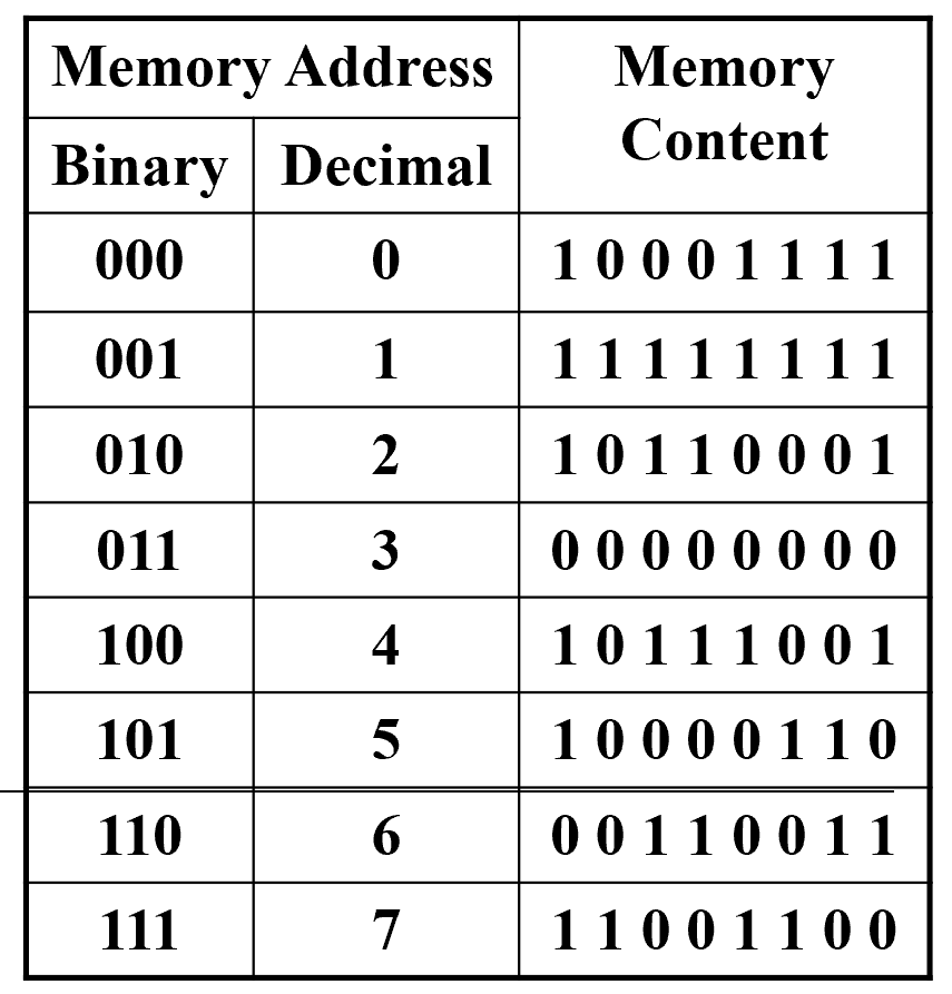
3 个地址位,\(0~7\), 每个地址存了 8 位数据,因此字长是 8.
Basic Memory Operations
Memory operations require the following:
- Data ─ data written to, or read from, memory as required by the operation.
- Address ─ specifies the memory location to operate on. The address lines carry this information into the memory. Typically: \(n\) bits specify locations of \(2^n\) words.
- An operation ─ Information sent to the memory and interpreted as control information which specifies the type of operation to be performed. Typical operations are READ and WRITE. Others are READ followed by WRITE and a variety of operations associated with delivering blocks of data. Operation signals may also specify timing info.
- Read Memory ─ an operation that reads a data value stored in memory:
- Place a valid address on the address lines.
- Toggle( 切换 ) the memory read control line.
- Wait for the read data to become stable.
- Write Memory ─ an operation that writes a data value to memory:
- Place a valid address on the address lines and valid data on the data lines.
- Toggle the memory write control line.
- Read Memory ─ an operation that reads a data value stored in memory:
Memory Operation Timing
- Most basic memories are asynchronous
- Controlled by control inputs and address
- Timing of signal changes and data observation is critical to the operation
-
Read timing

data valid 是等待的时间,随着数据大小、内存工艺不同,会花费不同的时间
-
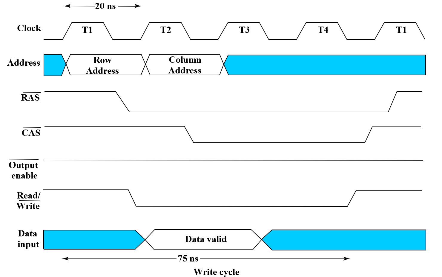
Write timing
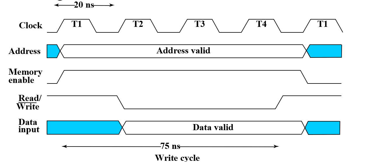
在 R/W 信号下降时要将 addr 锁存起来,上升时要预先把数据准备好。
RAM
Types of random access memory
- Static – information stored in latches
- Dynamic – information stored as electrical charges on capacitors
密度可以做的很高- Charge “leaks” off
- Periodic refresh of charge required
Dependence on Power Supply
- Volatile – loses stored information when power turned off
- Non-volatile – retains information when power turned off
Static RAM (SRAM)
Cell and Slices
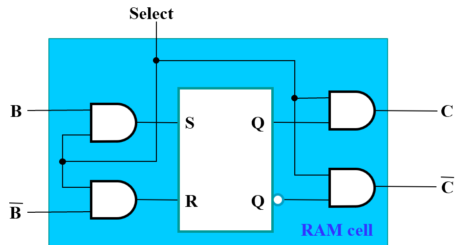
- SR Latch
- Select input for control 1
- Dual Rail Data Inputs \(B\) and \(\overline B\)
- Dual Rail Data Outputs \(C\) and \(\overline C\)
这里 Bit Select 的信号(每一个 Cell 都有
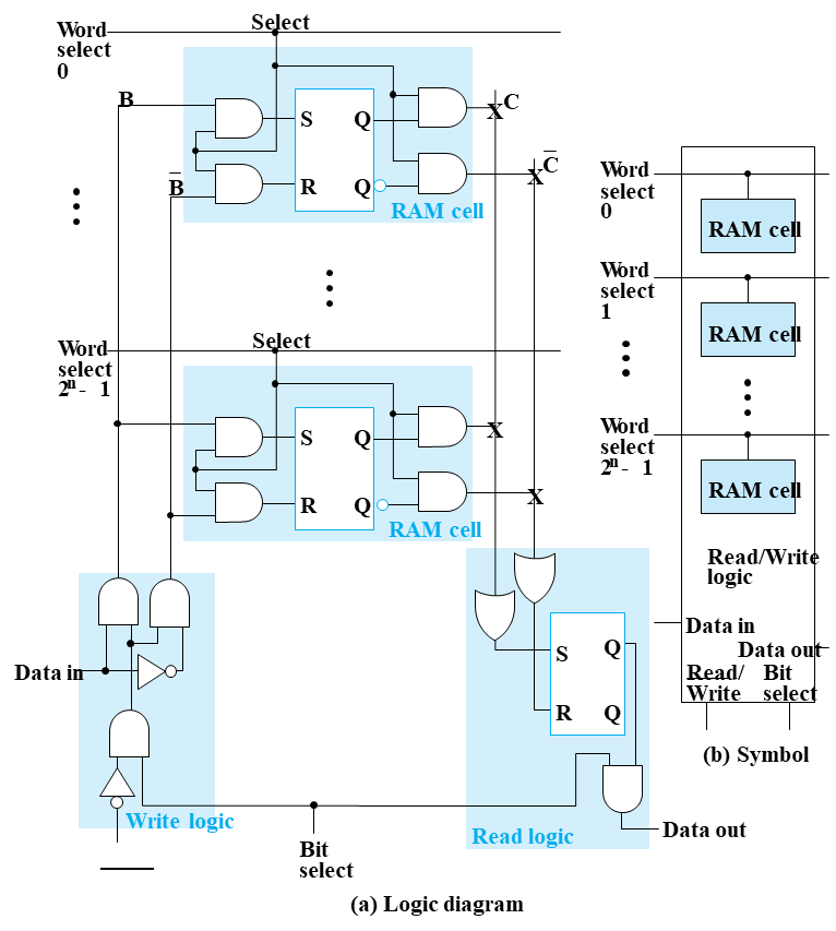
Cell Arrays and Coincident Selection
- Decoder - decodes the \(n\) address lines to \(2^n\) word select lines
将对应地址上的 Cells 的 Bit Select 信号置为 1 其余为 0. - A 3-state buffer on the data output permits RAM ICs to be combined into a RAM with \(c \times 2^n\) words
行列译码
- Word select becomes Row select
- Bit select becomes Column select

\(8\times 2\) RAM
Making Larger Memories
利用 CS 引脚,可以将 RAM 芯片拼起来

高位输入用来选择 RAM 芯片(输出是高阻态

Making Wider Memories
增加位宽,每块 RAM 芯片就代表最后输出的某一位。
Dynamic RAM (DRAM)
Basic Principle: Storage of information on capacitors.
Charge and discharge of capacitor to change stored value
Use of transistor as “switch” to:
- Store charge
- Charge or discharge

成本低,因此芯片里可以高密度使用。
写数据时直接充放电即可;读取时,需要有电路判断电压高低,这时会消耗电荷,要将破坏性读转为非破坏性(将值写回去)
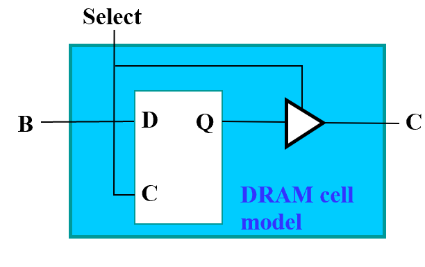
Cell and Slices
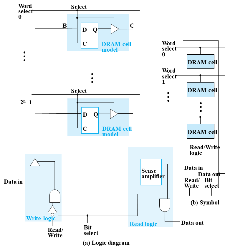
将所有的 DRAM 输出接到 Sense Amplifier 上,可以让破坏性读入变为非破坏性读入。
需要做定时刷新(电容会自己放电) - Refresh Controller and Refresh Counter
分别输入行地址、列地址(实际上是一组引脚,只是被 DRAM 分开输入
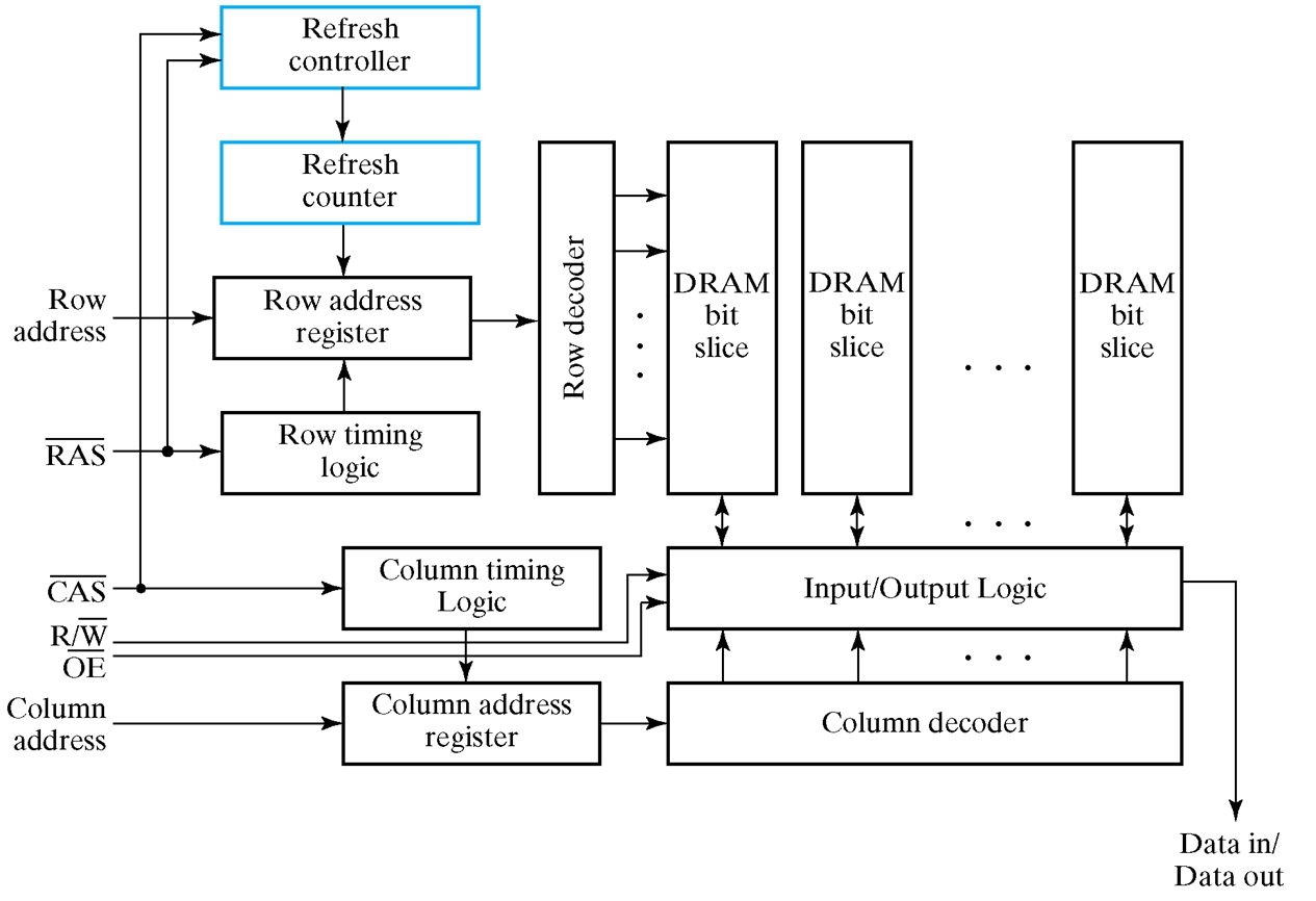
DRAM 是同步的,依赖时钟(SRAM 是异步)
- Read timing
- Write timing
DRAM Types
- Synchronous DRAM (SDRAM)
- Double Data Rate SDRAM (DDR SDRAM)
- RAMBUS® DRAM (RDRAM)
DRAM 存储量大,但相对 SRAM 操作会慢很多(还要分两个周期分别提供行地址和列地址)
-
Synchronous DRAM
Transfers to and from the DRAM are synchronize with a clock
Column address counter- for addressing internal data to be transferred on each clock cycle
- beginning with the column address counts up to column address + burst size – 1 一次可以读出多个数据
Synchronous DRAM - burst size=4

和 SRAM 配合形成 cache
-
Double Data Rate Synchronous DRAM
Transfers data on both edges of the clock
Provides a transfer rate of 2 data words per clock cycle - RAMBUS DRAM (RDRAM)
Uses a packet-based bus for interaction between the RDRAM ICs and the memory bus to the processor
The bus consists of:- A 3-bit row address bus
- A 5-bit column address bus
- A 16 or 18-bit (for error correction) data bus