Register and Register Transfers
约 3197 个字 31 张图片 预计阅读时间 11 分钟
Abstract
-
寄存器的概念、设计模型和结构
Register, Register Design Models- 门控时钟、并行加载控制
Registers with Clock Gating, Registers with Load-Controlled Feedback
- 门控时钟、并行加载控制
-
寄存器传输操作基本概念
Register transfer operations- 寄存器传输语言、基本微操作、条件传输原理、多寄存器传输的三种基本结构、原理和优缺点
Register Transfer Language (RTL), Microoperations, conditional transfer, three types of Register Transfer Structures: Multiplexer-Based Transfers, Bus-Based Transfers, Three-State Bus - RTL 与硬件描述语言的关系
Relationship of RTL and Verilog, implementation of conditional operations
- 寄存器传输语言、基本微操作、条件传输原理、多寄存器传输的三种基本结构、原理和优缺点
-
移位寄存器的概念、结构
Shift Registers- 串行输入、左移、右移、并行加载
serial input, shift left, shift right, parallel load
- 串行输入、左移、右移、并行加载
-
计数器的功能、类型
Function and type of counters- 纹波计数器的结构、工作原理、优缺点
Structure, theory, characteristic of ripple counter - 同步计数器的结构、工作原理、优缺点
Structure, theory, characteristic of synchronous counter - 进位链、并行进位、并行加载
carry chain, parallel carry, parallel load
- 纹波计数器的结构、工作原理、优缺点
-
采用同步时序电路设计方法设计模 n 计数器
Use the sequential logic model to designmodulo n counters - 采用输出结果反馈的方法设计模 n 计数器
Use output feedback model to design modulo n counters -
寄存器设计
RegisterDesign- 基于寄存器单元的设计方法,采用多路复用器设计
RegisterCellDesign,Multiplexer Approach - 基于时序电路设计方法的寄存器设计
Sequential Circuit Design Approach
- 基于寄存器单元的设计方法,采用多路复用器设计
-
串行传输和微操作
Serial Transfers and Microoperations
Registers
Register – a collection of binary storage elements
In theory, a register is a sequential logic which can be defined by a state table. More often, think of a register as storing a vector of binary values.
Example

如果有 \(n\) 位寄存器,需要 \(2^n\) 状态 . \(n\) 可能会很大,导致需要的状态,可能的输入组合、输出函数会很大。
Due to the large numbers of states and input combinations as n becomes large, the state diagram/state table model is not feasible!
- Add predefined combinational circuits to registers(e.g. To count up, connect the register flip-flops to an incrementer)
- Design individual cells using the state diagram/state table model and combine them into a register
把寄存器拆成单位的来设计,再考虑多位的拼接,最后组成多位寄存器。
Register Storage and Load Enable
Expectations:
- A register can store information for multiple clock cycles
- To “store” or “load” information should be controlled by a signal
但在刚刚的例子中,每个周期都会保存新的数据,不能做到在多个周期保留数据,因此是不行的。
Realizing expectations:
- Use a signal to block the clock to the register
- Use a signal to control feedback of the output of the register back to its inputs
- Use other SR or JK flip-flops, that for (0,0) applied, store their state
Load is a frequent name for the signal that controls register storage and loading
Load = 1: Load the values on the data inputs( 加载外部新数据 )Load = 0: Store the values in the register( 保持原有的数据 )
Solution
-
Registers with Clock Gating
The \(\overline{Load}\)(bar 表示低电平有效) signal enables the clock signal to pass through if 0 and prevents the clock signal from passing through if 1. (与 \(Load\) 相反)Example
For Positive Edge-Triggered or Negative Pulse Master-Slave Flip-flop:
\(Gated\ Clock = Clock + \overline{Load}\) 当 \(\overline{Load}\) 信号为 1 时,时钟信号不再随着外部时钟改变,这时就是保持原有的数据。
Clock Skew
问题在于我们是同步时序电路实现,要求时钟统一提供,这样所有的触发器会在同一时间完成操作。使用门控时钟的方式会带来更多的触发时间,时序电路从同步变为了异步的时序电路(触发有前有后) -
Registers with Load-Controlled Feedback
Run the clock continuously, and Selectively use a load control to change the register contents.Example

Register Transfer Operations
-
Register Transfer Operations – The movement and processing of data stored in registers
-
Three basic components:
- set of registers( 源寄存器,目标寄存器 )
- operations
- control of operations
- Elementary Operations -- load, count, shift, add, bitwise "OR", etc.
Elementary operations called microoperations
Register Notation
- Letters and numbers – denotes a register (e.g. \(R2, PC, IR\))
- Parentheses \((\ )\) – denotes a range of register bits (e.g. \(R1(1), PC(7:0), PC(L)\))
- Arrow \((\leftarrow)\) – denotes data transfer (e.g. \(R1 \leftarrow R2, PC(L) \leftarrow R0\)) H 代表高位 , L 代表低位 ( 如 \(PC(L),PC(H)\) 分别代表 \(PC\) 的高八位和低八位 )
- Comma – separates parallel operations
- Brackets \([\ ]\) – Specifies a memory address (e.g. \(R0 \leftarrow M[AR], R3 \leftarrow M[PC]\)) 寻址
Conditional Transfer

如果 \(K1=1\) 那么将 \(R1\) 的信号传给 \(R2\), 我们可以写为 \(K1:(R2\leftarrow R1)\), 其中 \(R1\) 是一个控制变量,表明条件执行的发生是否发生。
Register Cell Design
Assume that a register consists of identical cells.( 每个位执行相同操作 )
- Design representative cell for the register
- Connect copies of the cell together to form the register
- Applying appropriate "boundary conditions" to cells that need to be different and contract if appropriate
Specifications
- A register
- Data inputs to the register
- Control input combinations to the register
e.g. 控制输入 : Load, Shift, Add. 我们可以用三个引脚分别表示控制输入 (not encoded, one-hot code),也可以用两个引脚 S0 S1 的组合来表示控制输入 (encoded) - A set of register functions (typically specified as register transfers) 即规定控制输入的函数是对数据进行什么样的操作
- A hold state specification(e.g. If all control inputs are 0, hold the current register state)
Design
设计时,除了 Multiplexer Approach 还有 Sequential Circuit Design Approach
- Find a state diagram or state table
- Use the design procedure in Chapter 4 to complete the cell design
- For optimization:
- Use K-maps for up to 4 to 6 variables
- Otherwise, use computer-aided or manual optimization
Microoperations
Logical Groupings:
- Transfer - move data from one register to another
- Arithmetic - perform arithmetic on data in registers \(+-\times /\)
- Logic - manipulate data or use bitwise logical operations \(\wedge \vee \oplus \ \overline{x}\)
- Shift - shift data in registers
+
"+" 在逻辑表达式中表示或,在算术表达式中表示加法。
如 \((K1 + K2): R1 \leftarrow R1 +R3\), 左边为或,右边为加。
RTL, VHDL, Verilog Symbols for Register Transfers

Arithmetic Microoperations
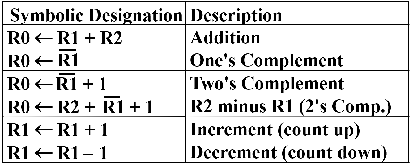
- Note that any register may be specified for source 1, source 2, or destination.
- These simple microoperations operate on the whole word
Logical Microoperations

Shift Microoperations
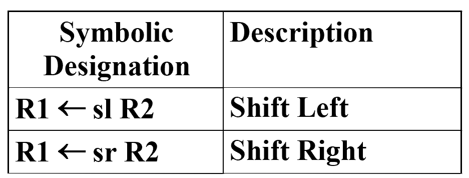
These shifts "zero fill". Sometimes a separate flip-flop is used to provide the data shifted in, or to “catch” the data shifted out.
Other shifts are possible (rotates, arithmetic).
Example
假设 \(R2=1100\ 1001\)
- \(R1 \leftarrow sl\ R2\) 之后 \(R2=1001\ 0010\)
- \(R1 \leftarrow sr\ R2\) 之后 \(R2=0110\ 0100\)
Register Transfer Structures
- Multiplexer-Based Transfers - Multiple inputs are selected by a multiplexer dedicated to the register
- Bus-Based Transfers - Multiple inputs are selected by a shared multiplexer driving a bus that feeds inputs to multiple registers
- Three-State Bus - Multiple inputs are selected by 3-state drivers with outputs connected to a bus that feeds multiple registers
- Other Transfer Structures - Use multiple multiplexers, multiple buses, and combinations of all the above
Multiplexer-Based Transfers
Multiplexers connected to register inputs produce flexible transfer structures (Note: Clocks are omitted for clarity)
Example
\(K1:R0\leftarrow R1\quad K2\overline{K1}:R0\leftarrow R2\)
我们可以将其化简: \(K1+K2\overline{K1}=K1+K2\) 就是 \(R0\) 寄存器会被更新时的控制逻辑. 并用 \(K1\) 作为 Mux 的选择信号。

完整电路(假设寄存器均为 4 位)

Multiplexer and Bus-Based Transfers for Multiple Registers
-
Multiplexer dedicated to each register

There can be three distinct registers as source, so can simultaneously do any three register transfers. (totally flexible)
如我们可以既可以实现 \(R0\leftarrow R1\) 也可以实现 \(R0\leftrightarrow R1\)
电路成本太高! -
Shared transfer paths for registers
A shared transfer object is a called a bus( 总线 )

A single bus driven by a multiplexer lowers cost, but limits the available transfers
不能同时 \(R0\leftarrow R1\) \(R1\leftarrow R0\)(类比:交换函数需要一个第三方变量)
Three-State Bus

Same simultaneous transfer capability as multiplexer bus
我们将寄存器和三态门封装在一起考虑,那么我们只需要一个外部引脚(n bits), 但多路复用器的方法需要两根位宽是 n 的引脚(因为三态门的外部引脚是可以双向传输数据的)
Shift Registers
Shift Registers move data laterally within the register toward its MSB or LSB position
In the simplest case, the shift register is simply a set of D flip-flops connected in a row like this:
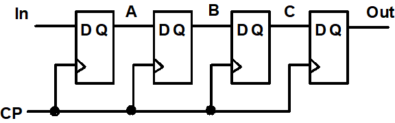
- Data input, In, is called a serial input or the shift right input.
- Data output, Out, is often called the serial output.
-
The vector (A, B, C, Out) is called the parallel output.
-
Parallel Load Shift Registers
By adding a mux between each shift register stage, data can be shifted or loaded
If SHIFT is low,\(D_A\) and \(D_B\) are replaced by the data on DA and DB lines, else data shifts right on each clock.
缺点: 没有数据保持操作,需要多添加一个选择项(3-1 选择)
Counters
Counters are sequential circuits which "count" through a specific state sequence. They can count up, count down, or count through other fixed sequences. Two distinct types are in common usage:
- Ripple Counters
- Clock connected to the flip-flop clock input on the LSB bit flip-flop
- For all other bits, a flip-flop output is connected to the clock input, thus circuit is not truly synchronous!
- Output change is delayed more for each bit toward the MSB.
- Resurgent because of low power consumption
- Synchronous Counters
- Clock is directly connected to the flip-flop clock inputs
- Logic is used to implement the desired state sequencing
Ripple Counter
每个时钟周期,A 计数器翻转一次。当 A 处于下降沿的时候 B 会进行一次求反。

每个触发器的时钟,没有接在同一个系统时钟上,是一个异步时序电路。
Question
考虑 3 位触发器,理想上 \(C=B=A=1\) 后从全 1 立即变成全 0. 但因为门延迟,实际变化过程为 \(111-110-100-000\)

此外对于 \(n\) bits, 最坏时间延迟是 \(n\cdot t_{PHL}\), 速度会非常慢
Synchronous Counters
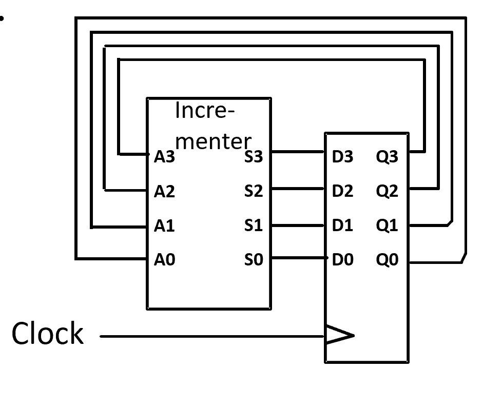
up-counter: incrementer \(S=A+1\)
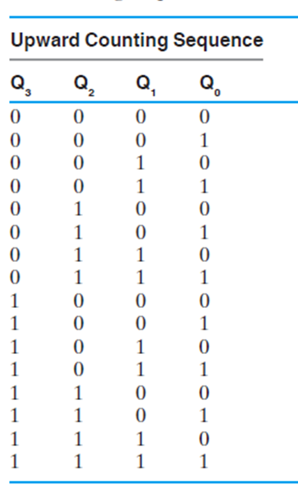
当位数增加,不利于化简设计。观察 \(Q_2\), 我们发现每次翻转的时候 \(Q_1,Q_0\) 均为 1. 类似在二进制计数器中 \(Q_n\) 只有在低 \(n-1\) 位均为 1 时才会取反。
我们可以用异或门,接在控制引脚和本位输出上,利用控制引脚来实现对本位输出的保持/取反。
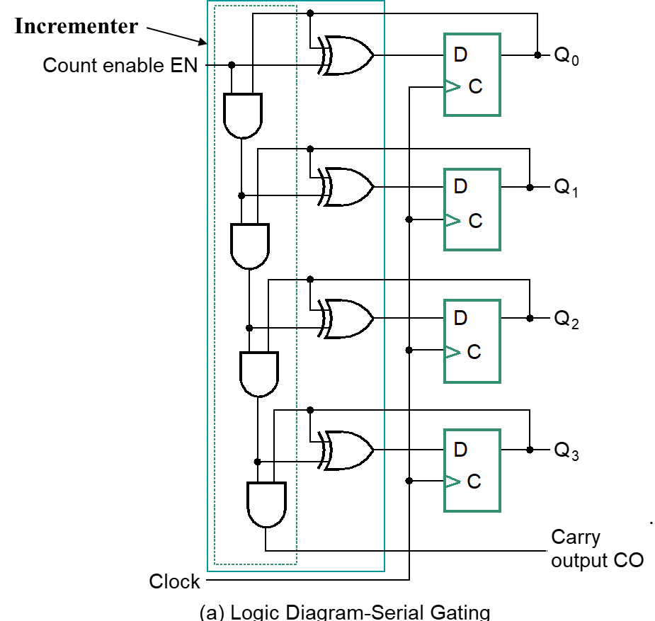
这里的控制信号是一个与门链,Count Enable 是与门链的使能Enable 为 0, 所有的与门链均为 0, 这时电路相当于是保持功能)
最后与门链输出一个 Carry Output, 表示所有位为 1 且 Enable=1. CO 是用于做级联(如两个四位计数器拼成一个八位计数器)接在后续计数器的 Enable 上。
存在问题:与门链是串接的,当计数器位数大时,与门链的传输延迟可能会影响计数器。
parallel gating:

Symbol for Synchronous Counter
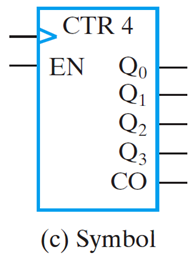
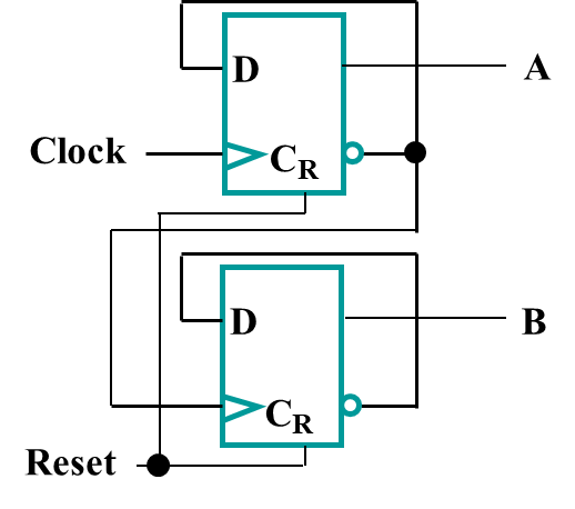
Other Counters - Counter with Parallel Load
在 D 输入触发器前加上 2-1 Mux( Load是选择信号 ), 选择与门链的结果 ( Load=0 ) or 外部输入 (Load=1 ),可以实现并行加载和计数的选择控制
| Load | Count | Action |
|---|---|---|
| 0 | 0 | Hold Stored Value |
| 0 | 1 | Count Up Stored Value |
| 1 | X | Load D |
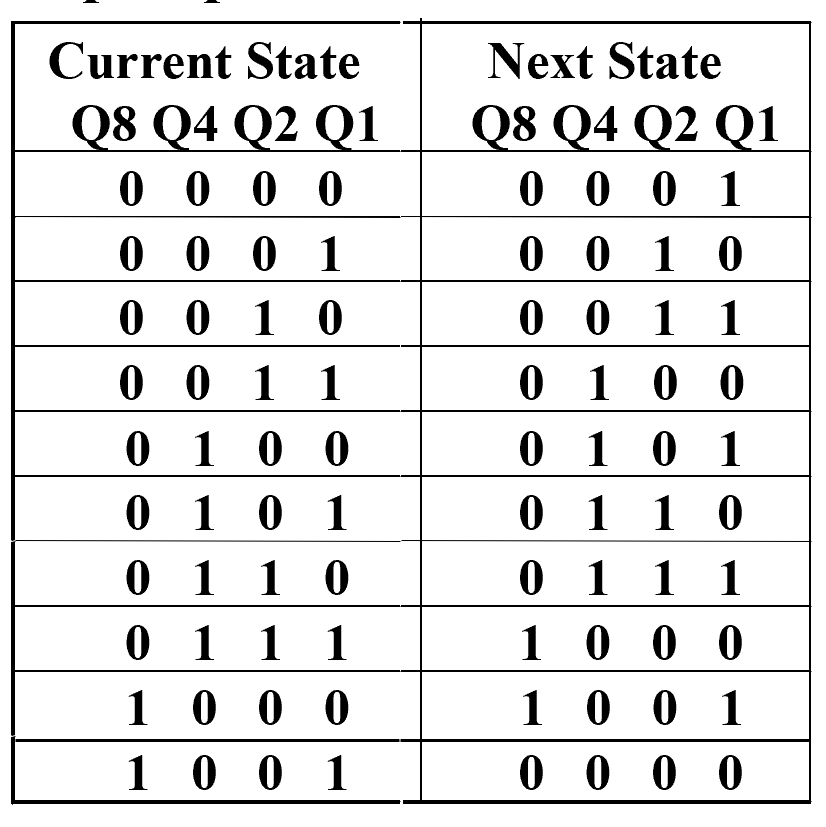
Design Example: Synchronous BCD
利用时序电路实现同步 BCD 计数器
-
状态表如下 :(1010-1111 don't cares)
-
基于上面的状态表,分别对 \(Q8,Q4,Q2,Q1\) 画卡诺图
利用卡诺图两级优化
- 画出电路图,添加复位引脚 (reset)
可以增加在触发器输入端(synchronous); 或者直接接在 D 触发器的异步复位 R 一端(asynchronous) - 如果电路因为干扰,跳到了无关态,能否恢复 ?
画出无关态的次态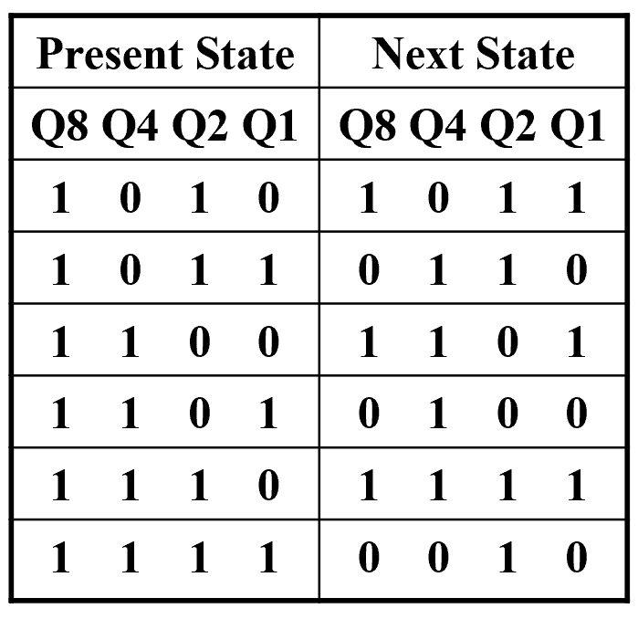
可以看到不会跳到异常状态后进入死锁,画出状态图如下

Other Counters - Counting Modulo N
BCD 码计数器就是模 10 计数器。 常用做法是将二进制计数器进行功能转换,利用同步/异步清零,加载功能,达到 \(N\) 时中止计数结果
-
检测值到达 N 后直接用异步清零引脚将计数器清零
Counting Modulo 7: Detect 7 and Asynchronously Clear

- A synchronous 4-bit binary counter with an asynchronous \(Clear\)( 异步复位脚,后同 ) is used to make a Modulo 7 counter.
- Use the \(\overline{Clear}\) feature to detect the count 7 and clear the count to 0. This gives a count of 0, 1, 2, 3, 4, 5, 6, 7(short)0, 1, 2, 3, 4, 5, 6, 7(short)0, etc.
但会短暂出现 7 这个状态,可能会带来干扰
- 检测值达到 \(N-1\) 时利用同步清零的方式在下个周期上升沿将计数器清零
Counting Modulo 7: Synchronously Load on Terminal Count of 6

- A synchronous 4-bit binary counter with a synchronous load and an asynchronous \(Clear\) is used to make a Modulo 7 counter
- Use the Load feature to detect the count "6" and load in "zero". This gives a count of 0, 1, 2, 3, 4, 5, 6, 0, 1, 2, 3, 4, 5, 6, 0, ...
不会直接清零,而是在到达 \(N-1\) 的时候,在下个时钟上升沿将其清零
如果需要设计从某个中间值 ( 非零 ) 开始计数的计数器,只需要将每次复位赋的外部输入变为该数字即可 ( 如果是 mod 15, 可以不需要用与门,直接利用之前的
Carry Output即可 )
多位计数器
多位寄存器,分开设计,如设计时间,低位为模 10 计数器,高位为模 6 计时器,低位的 Carry Output 既作为低位的同步清零信号,又是高位的 Enable 信号 .
Serial Operations
串行:
寄存器一次只接受一个二进制位,如果传输 n 位需要 n 个时钟周期。
需要的引线数量少,两个设备之间只需要一条线和一条地线就可以了。而且因为引线少,我们可以让其时钟频率达到非常高。
e.g. 设备与设备之间常使用串行 ( 外设 ), USB, 以太网线
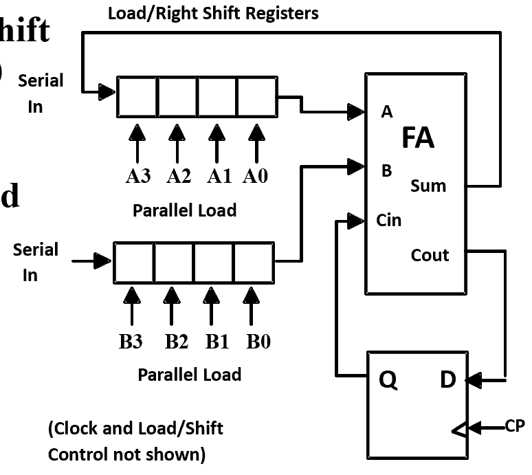
By using two shift registers for operands, a full adder, and a flip flop (for the carry), we can add two numbers serially, starting at the least significant bit.
Serial addition is a low cost way to add large numbers of operands, since a “tree” of full adder cells can be made to any depth, and each new level doubles the number of operands.
Other operations can be performed serially as well, such as parity generation/checking or more complex error-check codes.
Serial Adder