Combinational Logic Design
约 4133 个字 51 张图片 预计阅读时间 14 分钟
Abstract
- 组合电路定义(逻辑电路的两大类型:组合逻辑电路、时序逻辑电路)
Definition of Combinational Circuits - 模块与层次设计
Hierarchical Design - 逻辑事件的描述方法 *
Description of logic events - 逻辑门的主要参数
Technology Parameters
扇入(Fan-in)、扇出(Fan-out)、噪音容限(Noise Margin)、门的成本(Cost for a gate)、传输延迟(Propagation Delay) - 器件状态值或状态表与正逻辑,负逻辑的概念
Positive and Negative Logic - 三态门使用原则与总线(BUS)
BUS - 信号系统延时、延时模型、上升和下降时间、时钟上升和下降沿概念。
Delay Models, Positive and Negative Edge - 组合逻辑电路分析方法
Analysis of Combinational Circuits - 组合逻辑电路的设计方法
Design of Combinational Circuits - 函数与函数模块,基本逻辑功能
Functions and functional blocks - 计算机中的常用组合逻辑电路(功能芯片)
Frequently used Combinational Circuit in Computer Design
译码器、编码器、数据选择器(多路复用选择器)、数据分配器。 - 组合函数的实现技术
Implementing Combinational Functions Using:
译码器和或门
Decoders and OR gates
多路复用器(加反相器)
Multiplexers (and inverter) - 使能信号(EN,OE)的作用
Function of Enable Signal - 组合电路的迭代结构
Iterative combinational circuits - 算术函数:了解加、减、乘、除、增量函数及运算
Arithmetic function: Add, subtraction, multiplication, division, increment - 补码运算
2’s complement - 半加器及全加器函数及电路设计
Equations and Circuit implementation of 1 bit Half Adder and Full Adder - 多位全加器、全减器及设计
Design of multiple-bit Full Adder/ Subtracter - 超前进位:进位传递与延迟,进位函数:generate, Gi、propagate, Pi
Carry Lookahead: carry propagation and delay
Design Procedure
A combinational logic circuit has:
- A set of m Boolean inputs,
- A set of n Boolean outputs, and
- n switching functions, each mapping the \(2^m\) input combinations to an output such that the current output depends only on the current input values
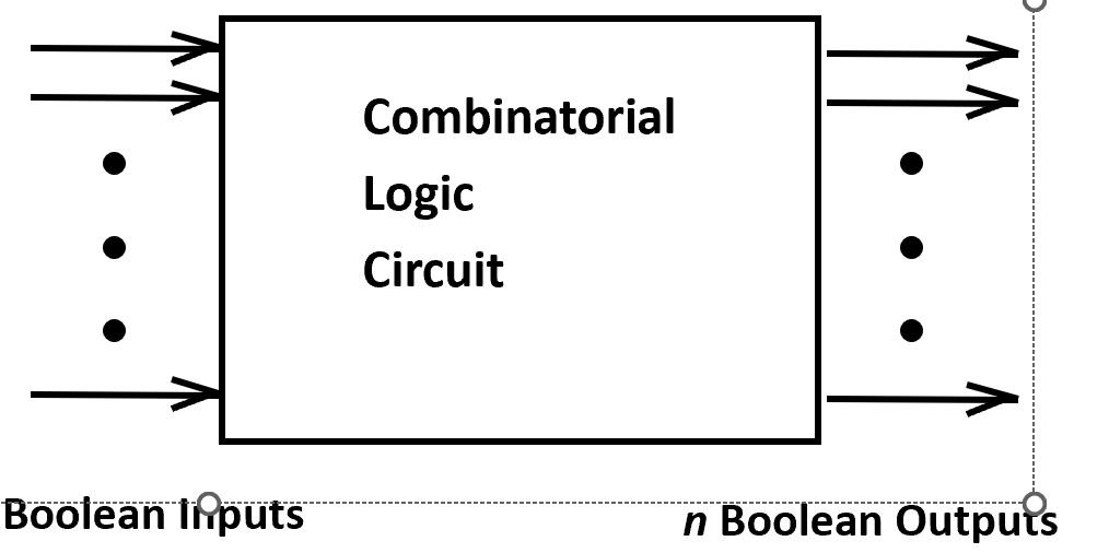
no state
Hierarchical Design
- Decompose the function into smaller pieces called blocks
- Decompose each block’s function into smaller blocks, repeating as necessary until all blocks are small enough
- Any block not decomposed is called a primitive block
- The collection of all blocks including the decomposed ones is a hierarchy
e.g.
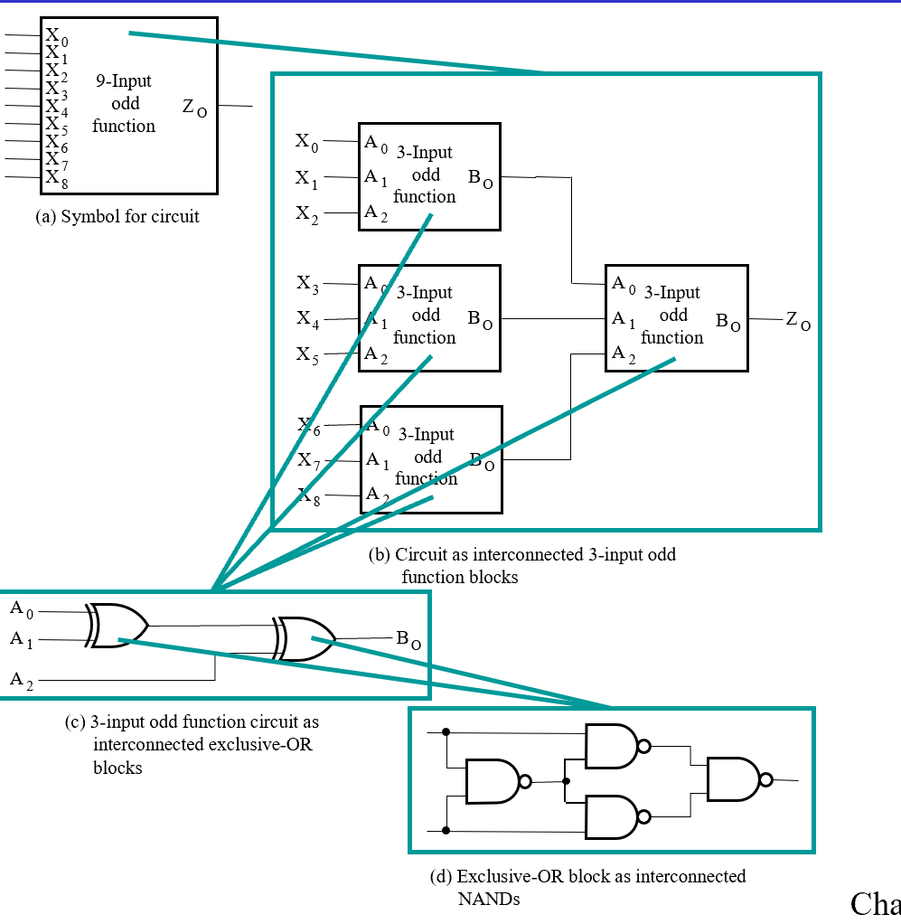
实例化模块和函数调用的区别
电路上实例化模块:复制一块并嵌入到电路中。且同时实例的模块是同时在运行,如上图中四个实例化的奇函数模块
但 C 语言函数体只有一份代码,只是 PC 跳到函数部分。
Reusable Functions:
把常用的操作抽象成模块,并提前定义好延迟等等特性。当需要使用时,我们把电路引脚接入即可。
Top-Down versus Bottom-Up
- A top-down design proceeds from an abstract, high-level specification to a more and more detailed design by decomposition and successive refinement
- A bottom-up design starts with detailed primitive blocks and combines them into larger and more complex functional blocks
Design Procedure
- Specification
Write a specification for the circuit if one is not already available -
Formulation
- Derive a truth table or initial Boolean equations that define the required relationships between the inputs and outputs, if not in the specification
-
Apply hierarchical design if appropriate 3. Optimization
-
Apply 2-level and multiple-level optimization
- Draw a logic diagram or provide a netlist for the resulting circuit using ANDs, ORs, and inverters
-
Technology Mapping
Map the logic diagram or netlist to the implementation 为什么需要这步?
很多时候需要用预先定义好的与非门,或者其他基本模块(如 XOR)直接套入电路中去,可以降低电路的成本和延迟。 technology selected - Verification Verify the correctness of the final design manually or using simulation.(仿真)
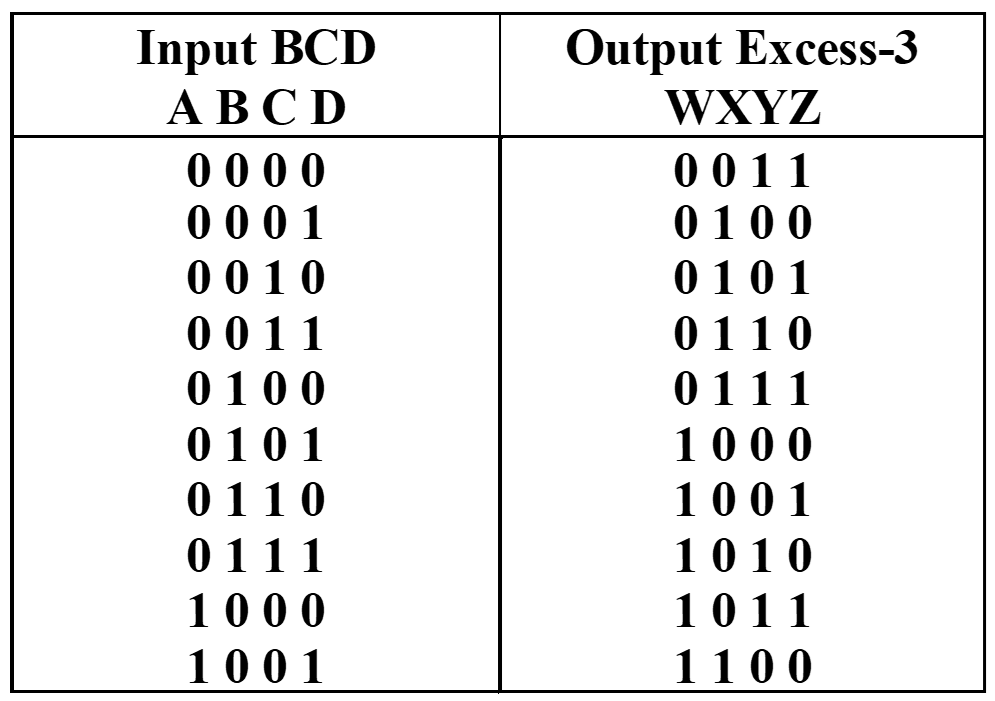
BCD to Excess-3 code converter
-
Specification
- Transforms BCD code for the decimal digits to Excess-3 code for the decimal digits
- BCD code words for digits 0 through 9: 4-bit patterns 0000 to 1001, respectively
其他输入认为是无关项。 - Excess-3 code words for digits 0 through 9: 4-bit patterns consisting of 3 (binary 0011) added to each BCD code word
- Implementation:
- multiple-level circuit.
- NAND gates(including inverters)
-
Formulation
-
Optimization
- two-level
W X Y Z 输出也需要四个逻辑函数。
单独 ABCD 四输入 对应一个输出 W, 用卡诺图化简。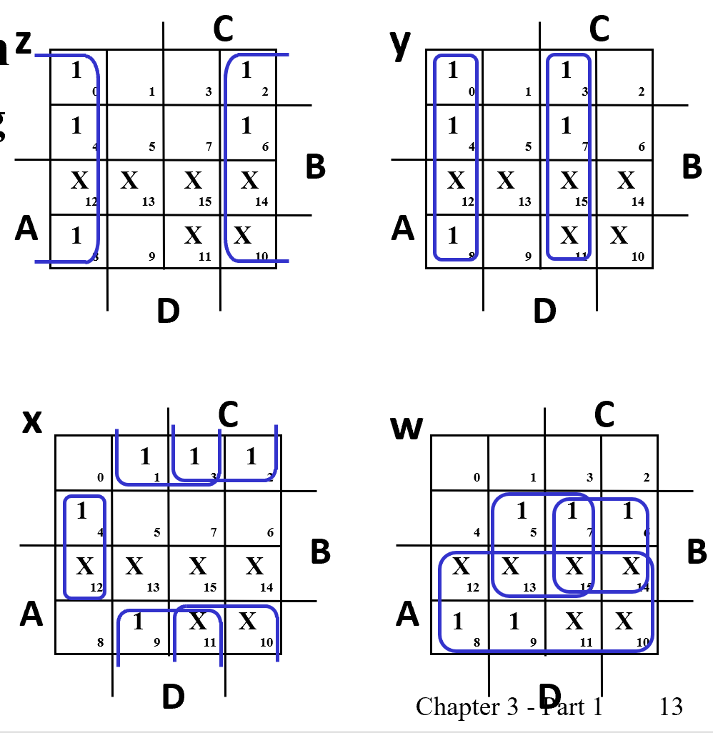
得到 \(W=A+BC+BD, X=\overline B C+\overline B D+B \overline C\overline D, Y=CD+\overline C\overline D, Z=\overline D\)
- multiple-level
\(G=7+10+6+0=23\).
优化后: \(T_1=C+D, W=A+BT_1, X=\overline B T_1B \overline C\overline D, Y=CD+\overline C\overline D, Z=\overline D\)
\(G=2+4+7+6+0=19\), 最多是三级电路。 \(\overline C\overline D=\overline{C+D}=\overline{T_1},T_1=C+D, W=A+BT_1, X=\overline B T_1B \overline C\overline D, Y=CD+\overline C\overline D, Z=\overline D\)
\(G = 2 +1 + 4 + 6 + 4 + 0 = 17\),最多是四级电路。 为什么要算 T1 非:ABCD 是外部输入的引脚,一般同时有原变量和反变量。但 T1 是内部产生的信号,对这个信号的非要自己计算得到。
- two-level
-
Technology Mapping
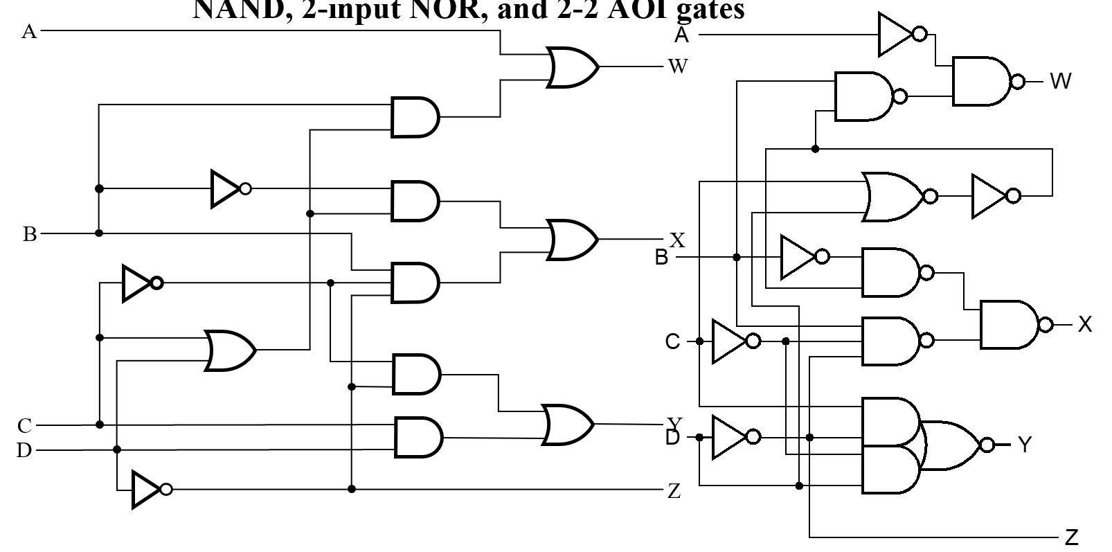
Mapping with a library containing inverters and 2-input NAND, 2-input NOR, and 2-2 AOI(与或非) gates
-
Verification
( 为什么有的时候算 G, 有的时候算 GN. 因为触发器同时有原变量和反变量,所以很多时候不需要单独算 GN.)
Chip Design Styles
- Full custom: 全部自己定制化,不用先定义好的模型
。 (因为库会考虑通用性,完整,带来成本开销比较高,延迟也相对大)
这种实现方式,研发成本高,但生产成本最低。 用于高性能,或者生产量非常大的时候。 Justifiable only for dense, fast chips with high sales volume. - Standard cell: 使用预先规定好的标准库 ( 如几输入的与门 )
- Gate array: 研发成本低。买现成的芯片,写进代码即可执行。成本最低(不用流片)
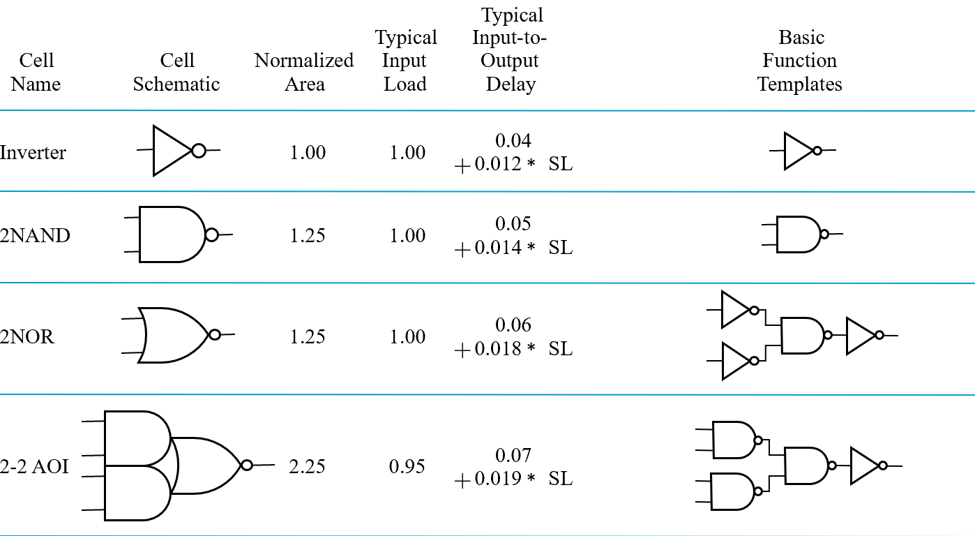
Cell Libraries
- Cell - a pre-designed primitive block
- Cell library - a collection of cells available for design using a particular implementation technology
- Cell characterization - a detailed specification of a cell for use by a designer - often based on actual cell design and fabrication and measured values
包括原理图,芯片面积,输入负载,延迟,工艺映射的模板库,硬件描述语言如何实现。
e.g.
Mapping to NAND gates
如何只用 NAND/NOR 做工艺映射
假设:不考虑 gate loading 和 delay. 可以有任意输入的与非/或非门。
The mapping is accomplished by:
- Replacing AND and OR symbols
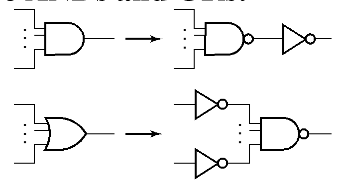
- Pushing inverters through circuit fan-out points
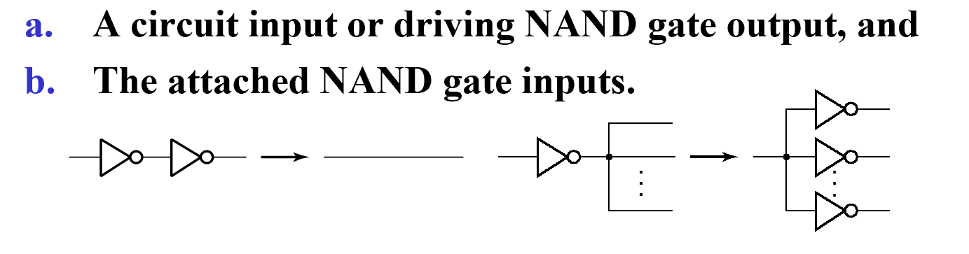
- Canceling inverter pairs
Example
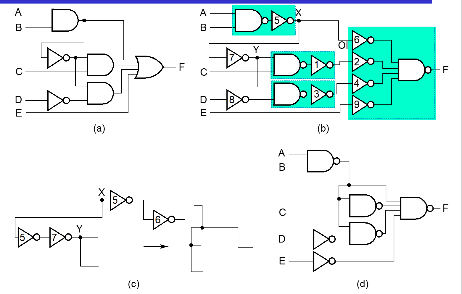
b -> c 就是把 5 推出散出点,随后和其他非门相消。
NONR 与 NAND 基本相同,除了 replace 这步。
Verification
验证方法:真值表 / 仿真 / 逻辑函数
小细节:仿真输出中有小脉冲,因为延迟产生。如果没有惯性延迟,我们要考虑把它吸收掉。
Behaviour Simulation 看不到,因为他不考虑传输延迟。多考虑使用有延迟的仿真
Combinational Logic
functional block: 偏高层逻辑应用,如译码器,选择器。
Rudimentary Logic Functions
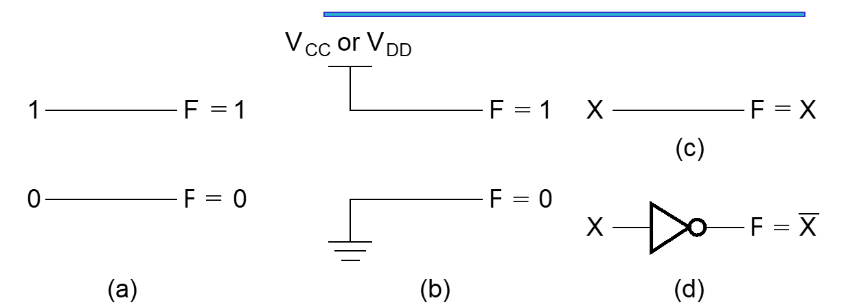
b 中表示接地和接电源。
Multiple-bit Rudimentary Functions
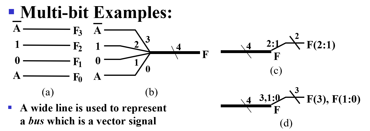
A wide line is used to represent a bus which is a vector signal.
b 中 4 表示位宽,4 位信号。
- Sets of bits can be split from the bus as shown in © for bits 2 and 1 of F.
- The sets of bits need not be continuous as shown in (d) for bits 3, 1, and 0 of F.
Enabling Function
- Enabling permits an input signal to pass through to an output
- Disabling blocks an input signal from passing through to an output, replacing it with a fixed value
The value on the output when it is disable can be Hi-Z (as for three-state buffers and transmission gates), 0 , or 1
Example
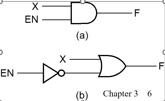
(a) when disabled, 0 output
(b) when disabled, 1 output. 其中也可以写 \(\overline {EN}\) 然后直接接或门,不用标 inverter.
Decoding
- Decoding - the conversion of an n-bit input code to an m-bit output code with \(n \leq m\leq 2^n\) such that each valid code word produces a unique output code.
- Circuits that perform decoding are called decoders.
3-8 译码器
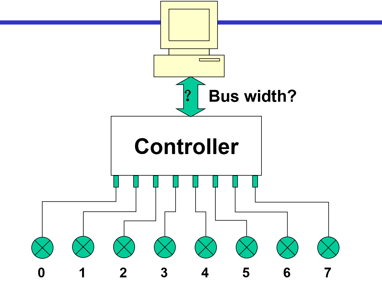
其真值表:
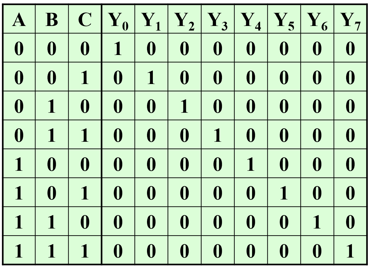
Example

朴素实现 n-to-m 的译码器有 \(n\times m\) 门输入成本.(\(2\times 2^n\))
译码器常用于内存,接在地址总线。 \(32-2^{32}\) 译码 . 成本 \(32\times 2^{32}\)
如何减少实现成本?
Decode Expansion
3-8 译码器,输入分成两部分,A 用 1-2 译码器 , B C 用 2-4 译码器
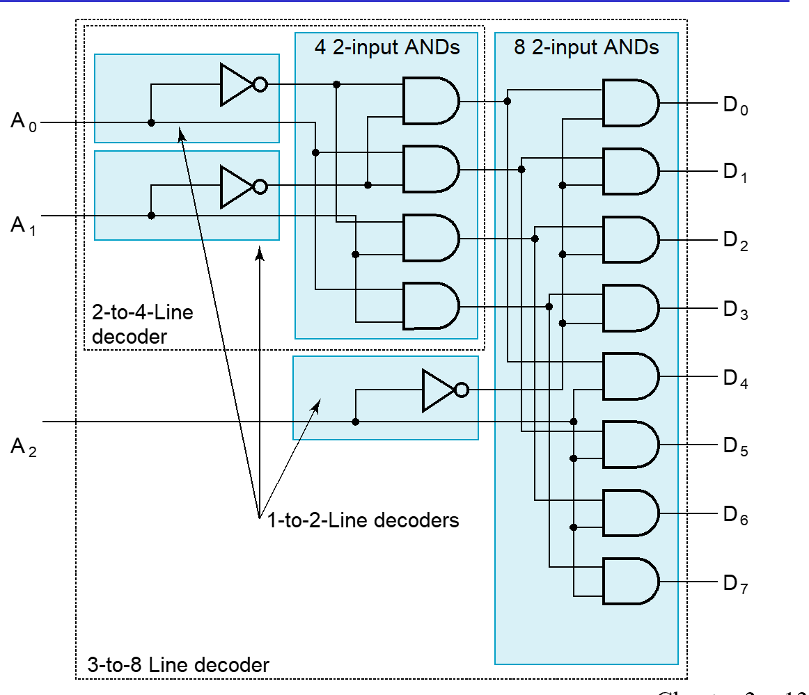
抽象为行列译码:一组是行译码,一组是列译码。 对于 \(n - 2^n\) 设计两个译码器,一个 \(\dfrac{n}{2}\) 输入 \(2^{\frac{n}{2}}\) 的行译码器,一个 \(\dfrac{n}{2}\) 输入 \(2^{\frac{n}{2}}\) 输出的列译码器。
这样再把行列的输出用 2-AND 连接,我们只需要 \(2^{\frac{n}{2}}\times 2^{\frac{n}{2}}=2^n\) 个 AND 门 , 中间与门阵列的成本是 \(2^n\times 2 =2^{n+1}\).
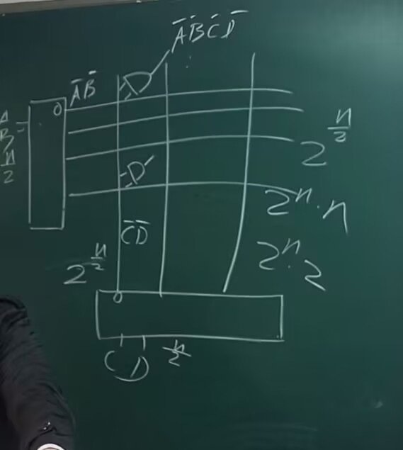
译码延迟加大,但降低成本。
Decoder with Enable
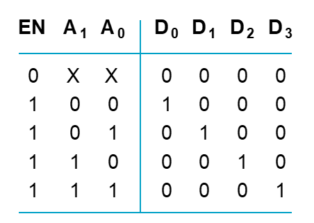
Note
Alternatively, (b) can be viewed as distributing value of signal EN to 1 of 4 outputs
In this case, called demultiplexer( 分配器 ).
把 D1 看作 D1=EN. 即 \(A_1, A_0\) 决定把 EN 的信号分配到哪个引脚。
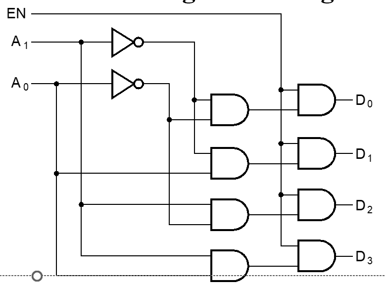
Combinational Logic Implementation - Decoder and OR Gates
Implement m functions of n variables with:
- Sum-of-minterms expressions
- One n-to-2n-line decoder
- m OR gates, one for each output
把最小项或起来,得到任意的逻辑函数
Binary Adder
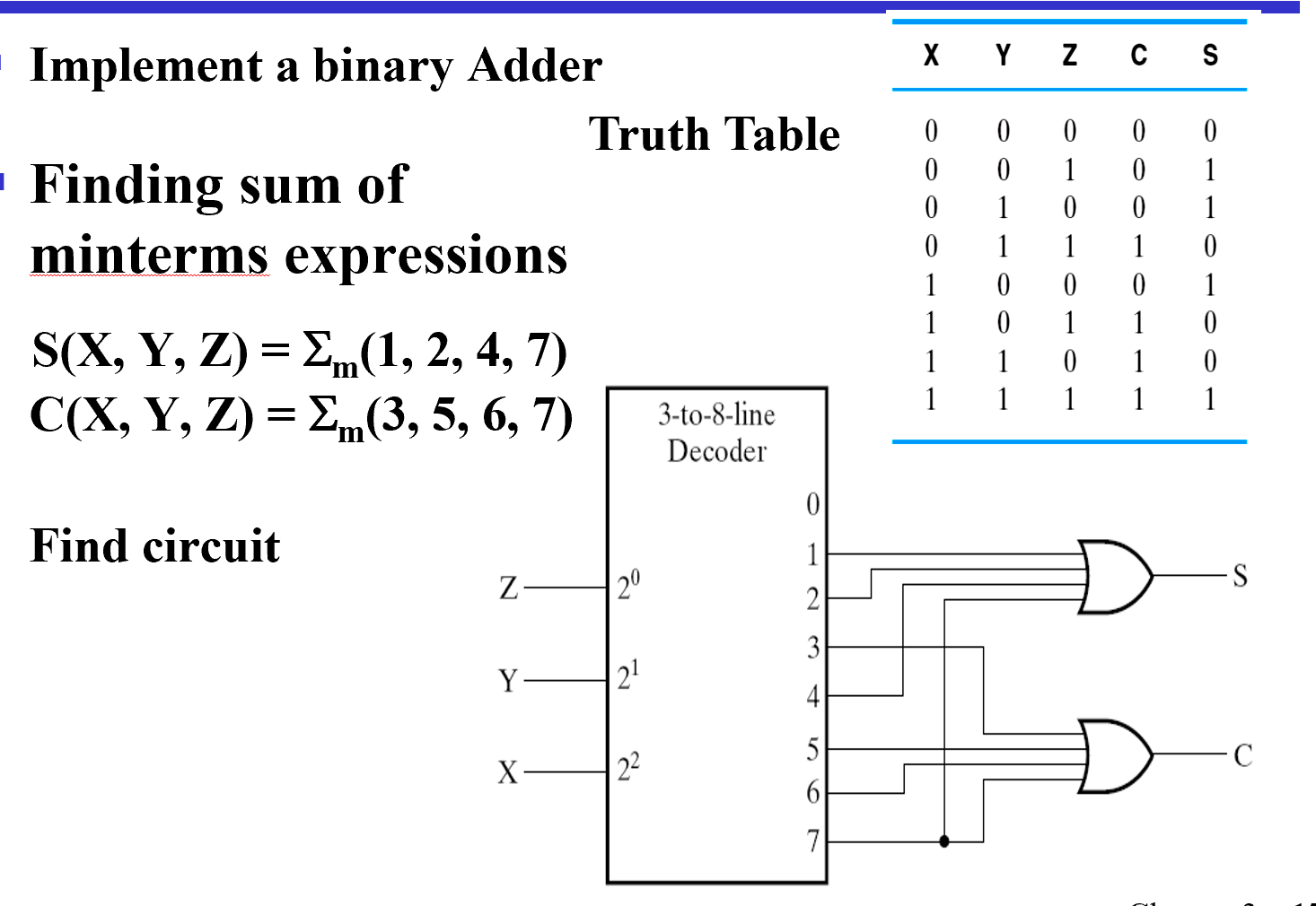
BCD-to-Segment Decoder
七段数码管里,亮不同的段即可表示不同的数字
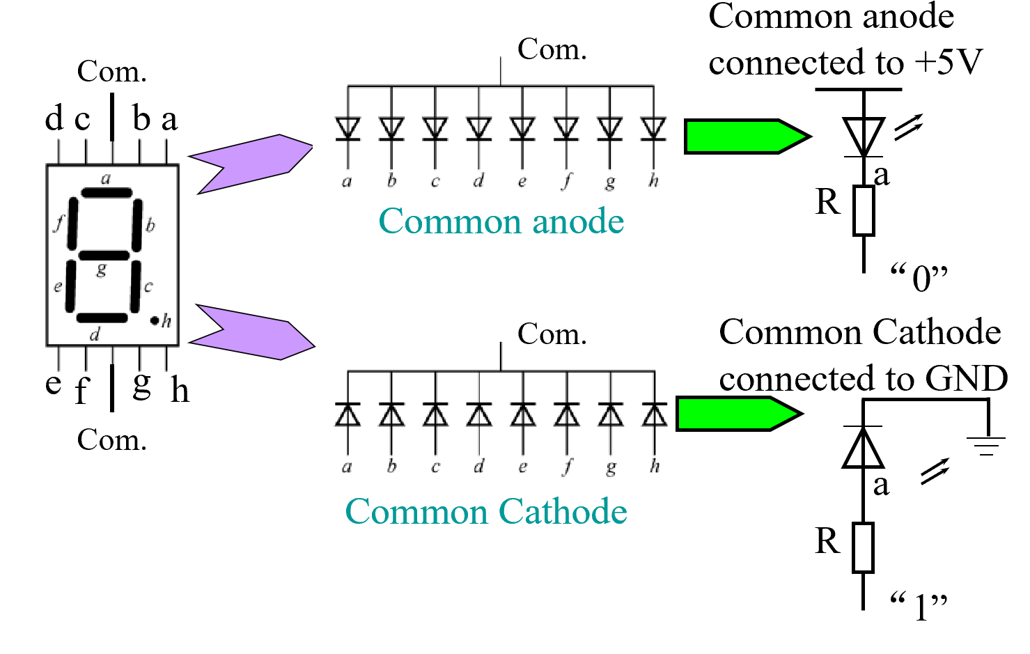
上为共阳极(输出 0 才能亮,阴极相反)下为共阴极
输入不同的数字,亮对应的数码管,使其可以显示在数码管上
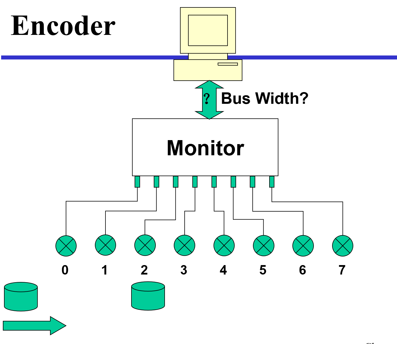
Encoding
Encoding - the opposite of decoding - the conversion of an m-bit input code to a n-bit output code with \(n <=m <= 2^n\) such that each valid code word produces a unique output code
一个译码器 \(2^n\) 输入,n 个输出。常用于中断信号,计算机响应,告诉 CPU 哪一号的中断发生了(这里就要进行编码)
decimal-BCD encoder
- Inputs: 10 bits corresponding to decimal digits 0 through 9, (D0, …, D9)
- Outputs: 4 bits with BCD codes
- Function: If input bit Di is a 1, then the output (A3, A2, A1, A0) is the BCD code for i.
A3 = D8 + D9;
A2 = D4 + D5 + D6 + D7;
A1 = D2 + D3 + D6 + D7;
A0 = D1 + D3 + D5 + D7 + D9
如果输入的 10 根线里,有两个输入都为 1, 可能会得到没有意义的输出,需要优先级。
Priority Encoder
如果这里有多个输入为 1, encoder 会将优先级最高的值编码。
Example
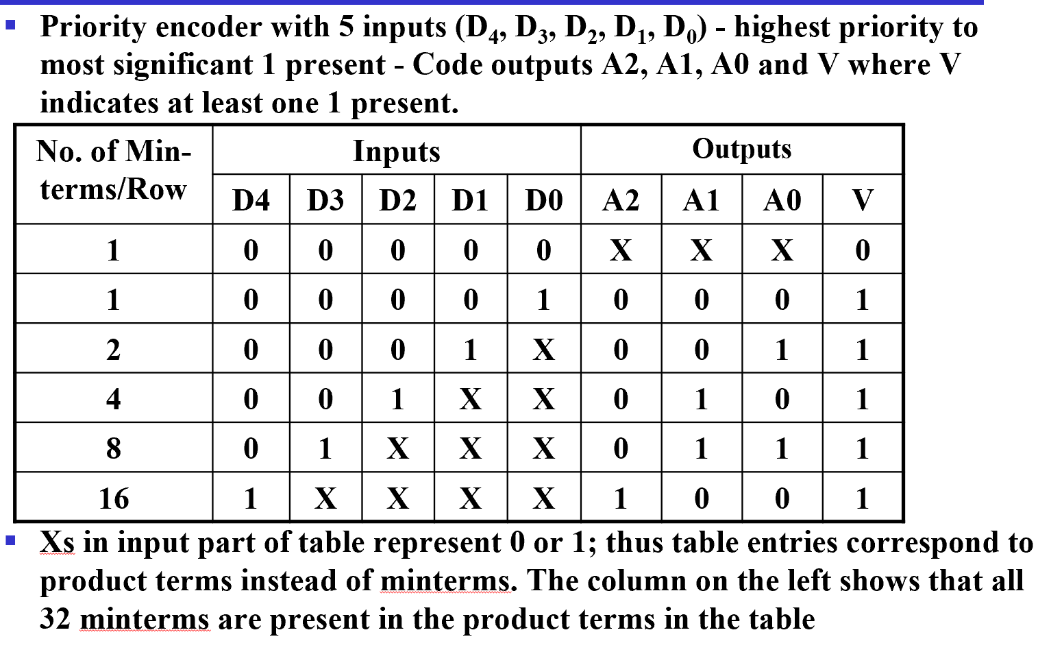
V 表示是是否有有效信号进入 \(A2 = D4\)
\(A1 = \overline{D4} D3 + \overline{D4} D2 = \overline{D4}F1, F1 = (D3 + D2)\)
\(A0 = \overline{D4} D3 + \overline{D4}\overline{D3}\overline{D2} D1 = \overline{D4} (D3 + \overline{D2} D1)\)
\(V = D4 + F1 + D1 + D0\)
Multiplexers
Circuits that perform selecting have:
- A set of information inputs from which the selection is made
- A single output
- A set of control lines for making the selection
Logic circuits that perform selecting are called multiplexers.
A typical multiplexer has n control inputs \((S{n - 1},... S_0)\) called selection inputs, \(2^n\) information inputs \((I_{2^n - 1}, … I_0)\), and one output Y.
如果输入 \(m<2^n\) 也可以设计为 n select lines 的 multiplexers.
2-to-1-Line Multiplexer
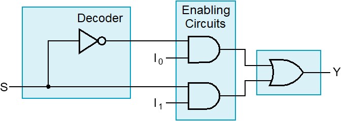
S = 0 时选择 \(I_0\); S = 1 时选择 \(I_1\).
Equation: \(Y=\overline S I_0+SI_1\)
画电路图时,要分成两块:第一部分 1-2 译码器,后一部分是 2-2 与或结构。(结构复杂后,其实就是将这两部分扩展)
In general, \(2^n\)-to-1-line multiplexers:
- n-to-\(2^n\)-line decoder
- \(2^n \times 2\) AND-OR
Example
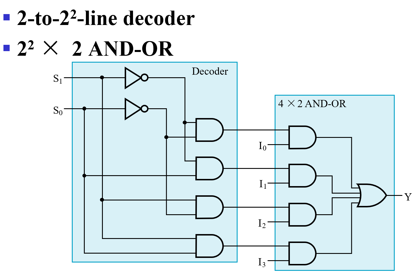
任何时刻译码器只有一个输出是 1, 相当于只有一个与门被 enable, 其余都 disable. 这样就能选择出 enable 的信号。
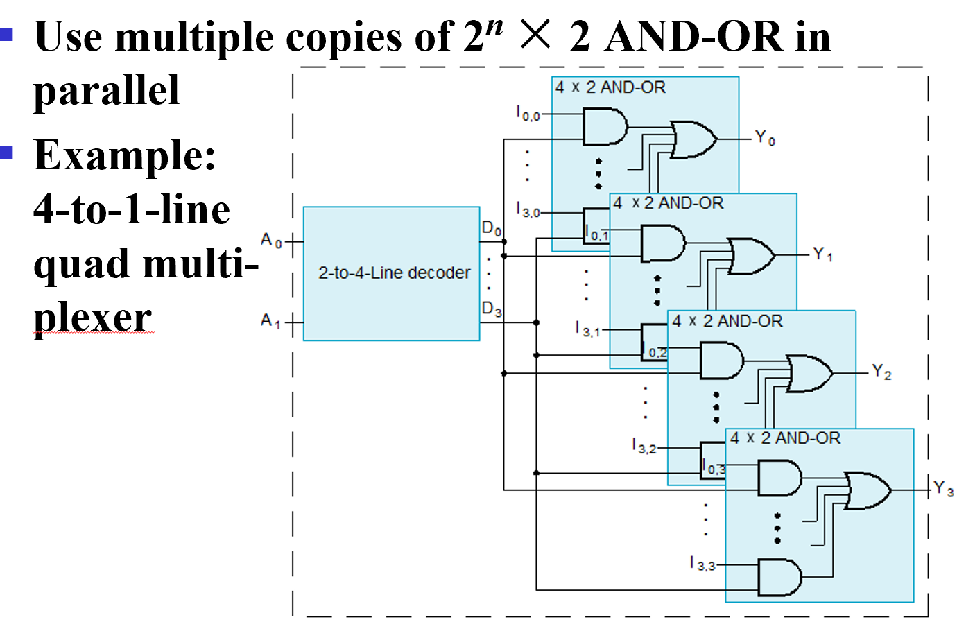
多位的数据选择。这里有四组信号,每组信号都是四个输入的一位,但选择逻辑对于四组信号是一样的,因此最后选出来的都是同一组信号。即最后输出的四位信号都来自同一根总线,
我们也可以不用与或结构,使用三态门实现 mux.
三态门改进 Mux
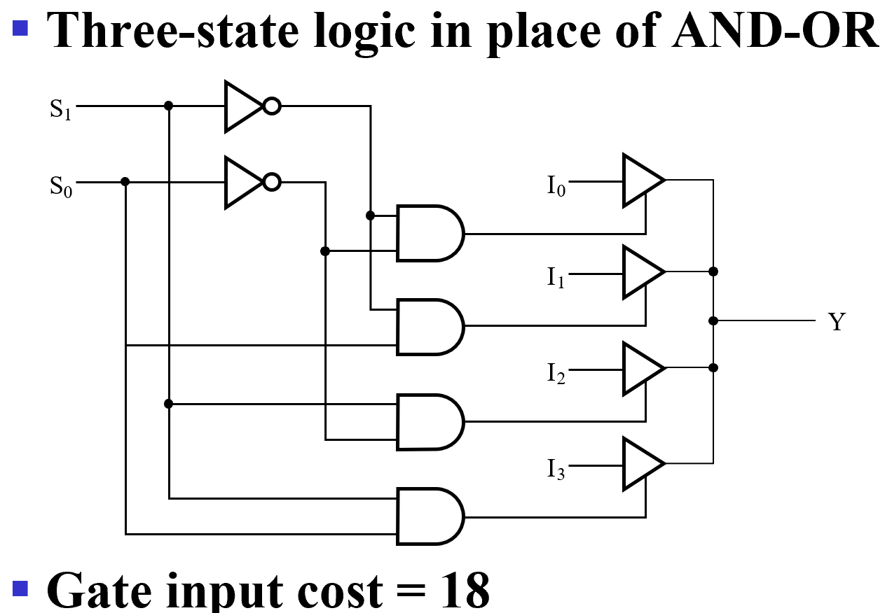
( 利用三态门可以将输出并在一起,同时最多只有一个三态门有有效输出。我们这里译码器只会有一个输出为 1, 保证了电路安全;这样还可以降低成本 )
我们还可以将译码器也使用三态门:
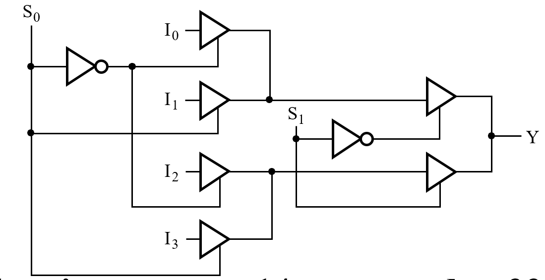
这里我们是两层选择的逻辑,S0 = 0 时先选出 I0(00) 和 I2(10), S1 再进行第二层的选择。
Combinational Logic Implementation- Multiplexer Approach
对于一个 n 变量的逻辑函数,我们可以把它抽象为 n 个输入对应一个输出。我们可以用 Mux 对应真值表中的 \(2^n\) 行的结果,用 n 输入作为选择线来查表。
Gray to Binary Code
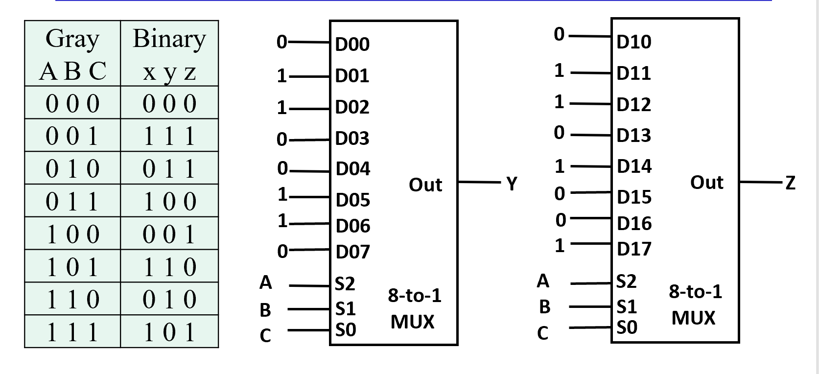
相当于利用 ABC 查表,如果 mux 选择出一位(根据真值表得到)
注意引脚顺序!
我们可以做进一步改进,\(n+1\) 变量用 \(2^n-1\) mux
对于 \(F(A,B,C)\) 当 A B 确定时,最后可能输出只可能为 \(1,0,C,\overline C\)
利用这点我们可以改造真值表,
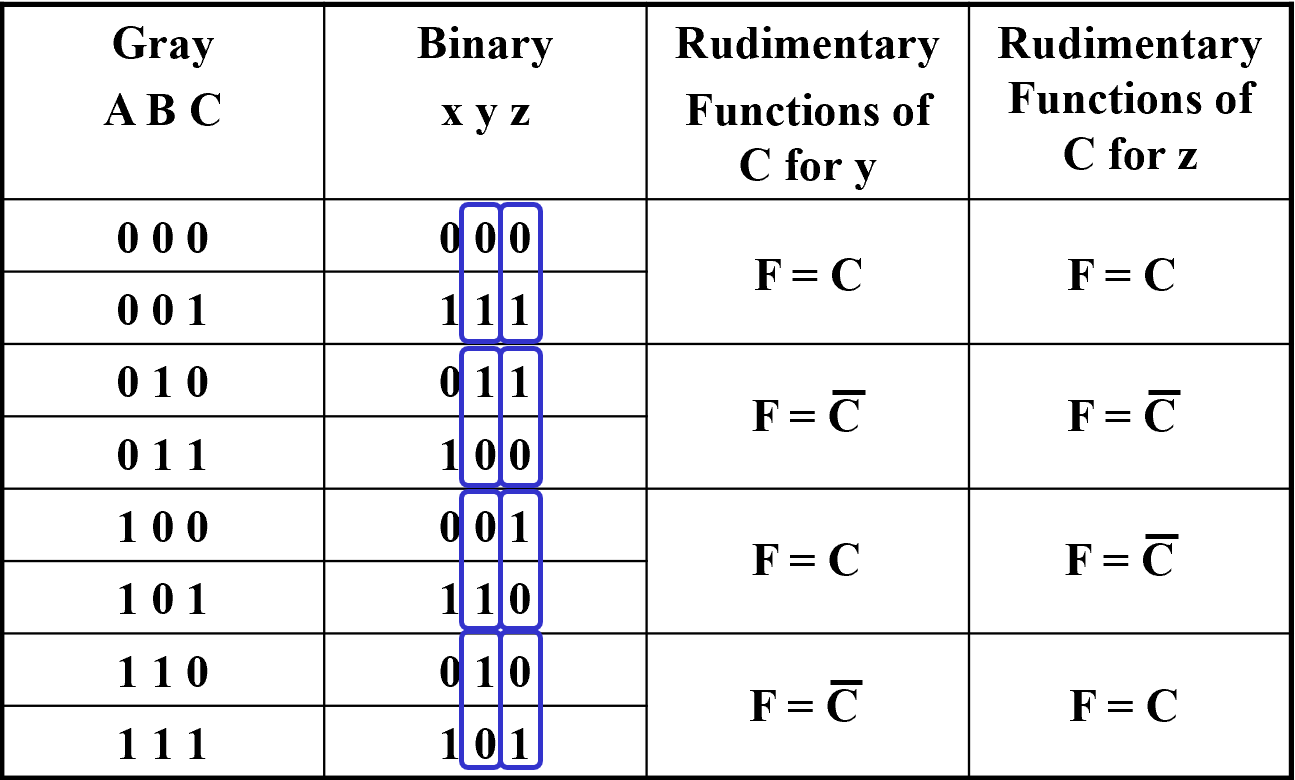
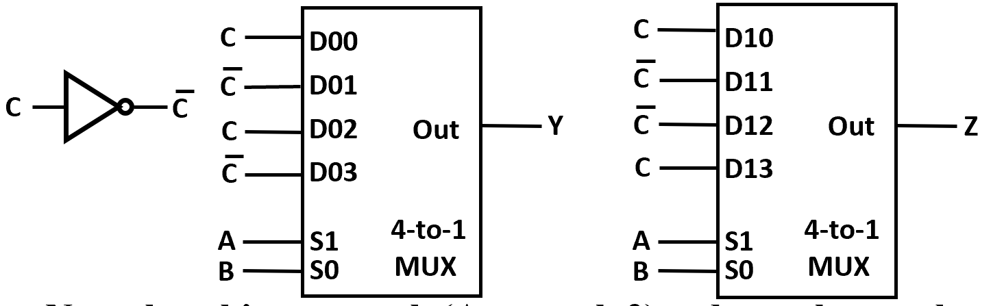
理论上还可以放更多变量到另一边
Arithmetic Functions
Cell - subfunction block 单元模块,处理每位
Functional Blocks: Addition
Addition Development:
- Half-Adder (HA), a 2-input bit-wise addition functional block.(no carry input)
- Full-Adder (FA), a 3-input bit-wise addition functional block.
- Ripple Carry Adder, an iterative array to perform binary addition.
- Carry-Look-Ahead Adder (CLA), a hierarchical structure to improve performance.
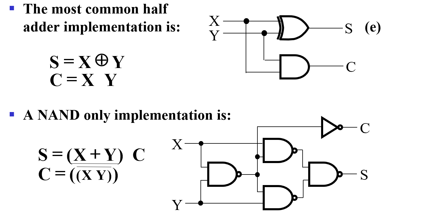
Half-Adder
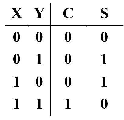
\(S=X\oplus Y, C=XY\).
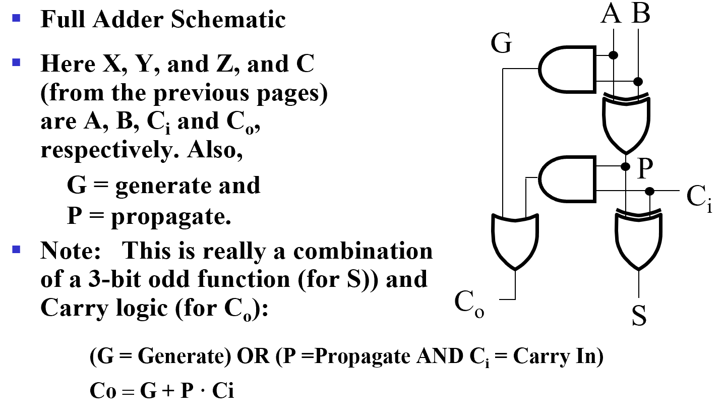
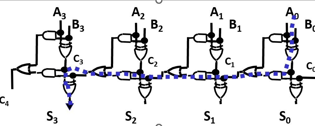
Full Adder
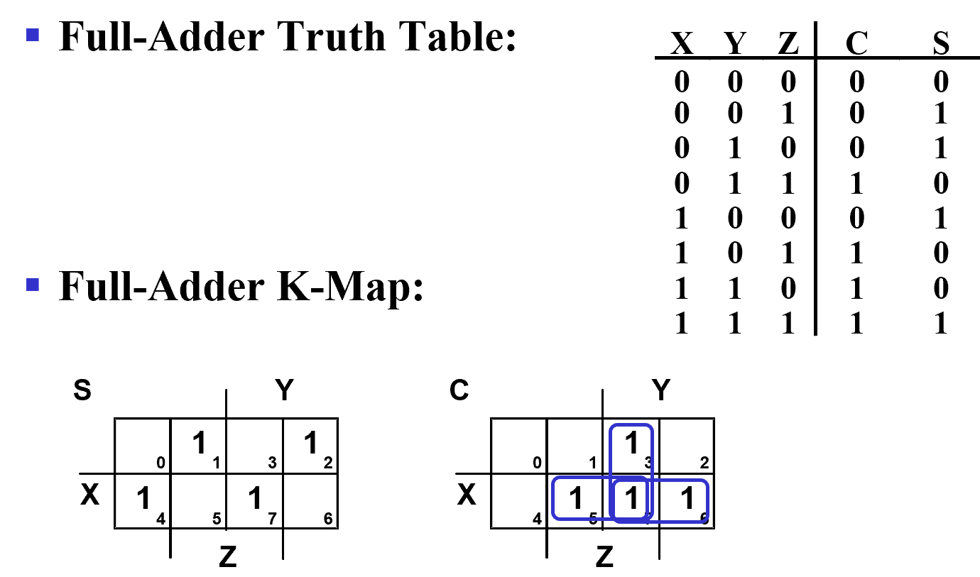
S 无法化简,但可以表示为奇函数(异或)
\(S=X\overline Y\overline Z+\overline X Y \overline Z + \overline X\overline YZ+XYZ=X\oplus Y\oplus Z\)
\(C=XY+XZ+YZ=XY+(X\oplus Y)Z\).
The term \(XY\) is carry generate.(\(XY=1\) 时一定会有进位 )
The term \(X\oplus Y\) is carry propagate.(\(X\oplus Y=1\) 时 X,Y 有一个是 0, 一定会把进位传下去,即 \(C=Z\))
Note
注意 C 的改写,这里改为异或不改变结果,同时因为已经有 xor 了,可以节约一个门。
Implementation:
Binary Adders
实现二进制多位加法
4-bit Ripple-Carry Binary Adder
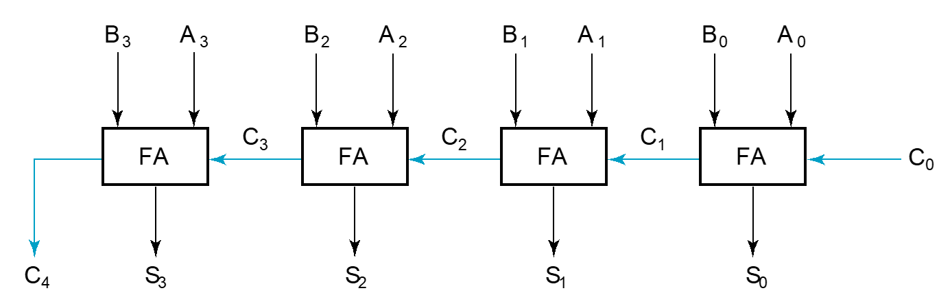
存在一个问题:随着加法器位数的增加,延迟会越来越大。
如下图中,最长的路径是从 A0 或 B0 到 S3.
Carry Lookahead
对于状态 i, 我们称 \(G_i\) 为 generate, \(P_i\) 为 propagate.
- \(G_i\), \(P_i\), and \(S_i\) are local to each cell of the adder
- \(C_i\) is also local each cell
全加器的更新可以定义为
这样 \(C_{i+1}\) 可以从 cells 中去掉,同时我们可以推导得到一组跨越多个单元的进位方程:
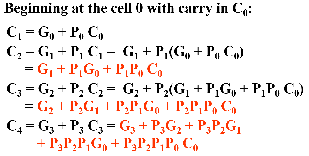
于是我们可以得到下面的 Carry Look-ahead Adder:
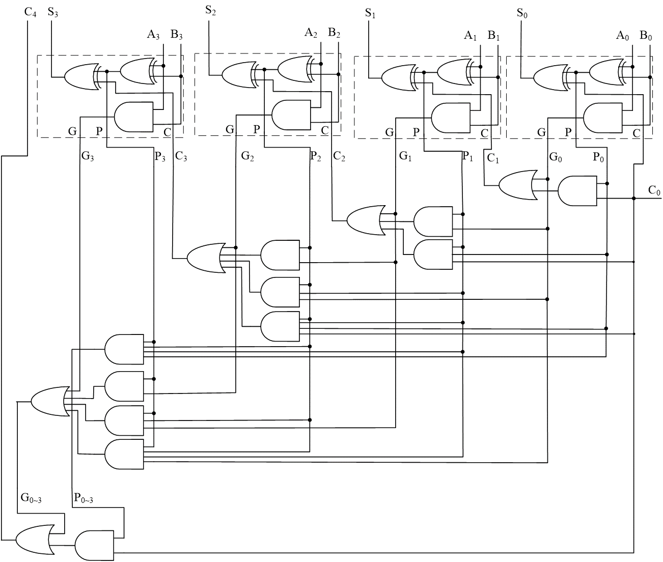
这样的超前进位全加器,避免了因为位过多而造成延迟过大。高位的结果直接由低位的结果得到。
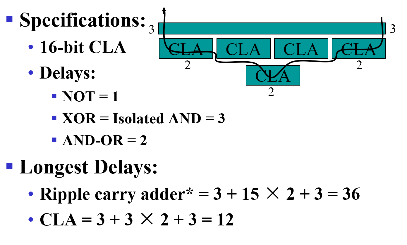
This could be extended to more than four bits; in practice, due to limited gate fan-in, such extension is not feasible.
The concept is extended another level by considering group generate(\(G_{0-3}\)) and group propagate(\(P_{0-3}\)) functions:
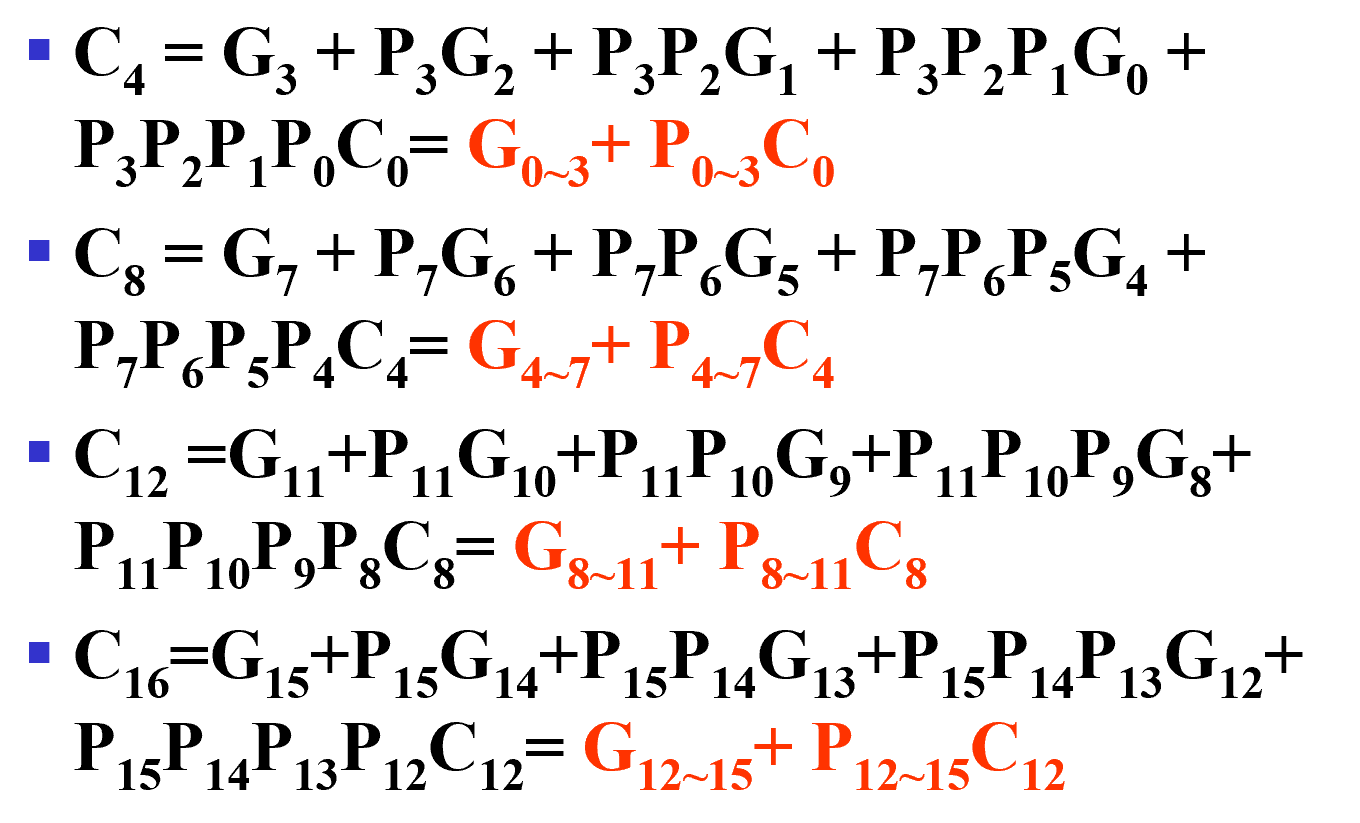
这样我们就得到了 16-bits adder
Exactly the same structure. So CLA could be used to generate Group Carry.
类似思路可得到 64 位的加法器。
Example
Unsigned Subtraction
- Subtract the subtrahend( 减数 ) N from the minuend( 被减数 ) M
- If no end borrow occurs, then \(M\geq N\), and the result is a non-negative number and correct.
- If an end borrow occurs, the \(N > M\) and the difference \(M - N + 2^n\) is subtracted from \(2^n\), and a minus sign is appended to the result.
To do both unsigned addition and unsigned subtraction requires:
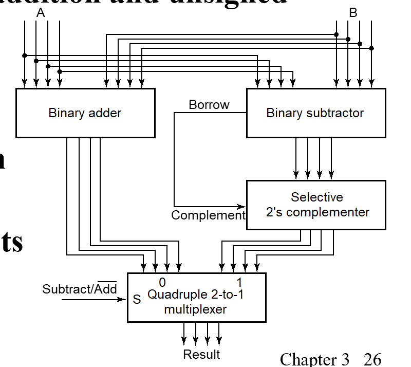
复杂,成本高
Complements
- Diminished Radix Complement of N 反码
defined as \(r^n-1-N\)(\(r^n-1\) 是 bits[n-1:0] 全为 1 的二进制数,用它减去 N 即可得到 N 按位取反的结果,即反码)
The 1's complement is obtained by complementing each individual bit (bitwise NOT). - 2’s complement 补码
defined as \(r^n-N\)
- 反码按位取反再加一
- 也可以这样求补码:从右往左第一个 1 之前不变,此后其他位全部求反
Subtraction is done by adding the complement of the subtrahend.
- Subtraction with 2’s Complement
- Add the 2's complement of the subtrahend N to the minuend M: \(M + (2^n -N) = M - N + 2^n\)
- if \(M\geq N\), the sum produces end carry \(r^n\) which is discarded; from above, \(M - N\) remains.
- If \(M < N\), the sum does not produce an end carry and, from above, is equal to \(2^n - ( N - M )\), the 2's complement of \(( N - M )\).
To obtain the result \((N – M)\), take the 2's complement of the sum and place a \(-\) to its left.
Example
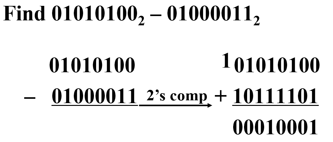
进位是 1 表明结果为正,不需对结果修正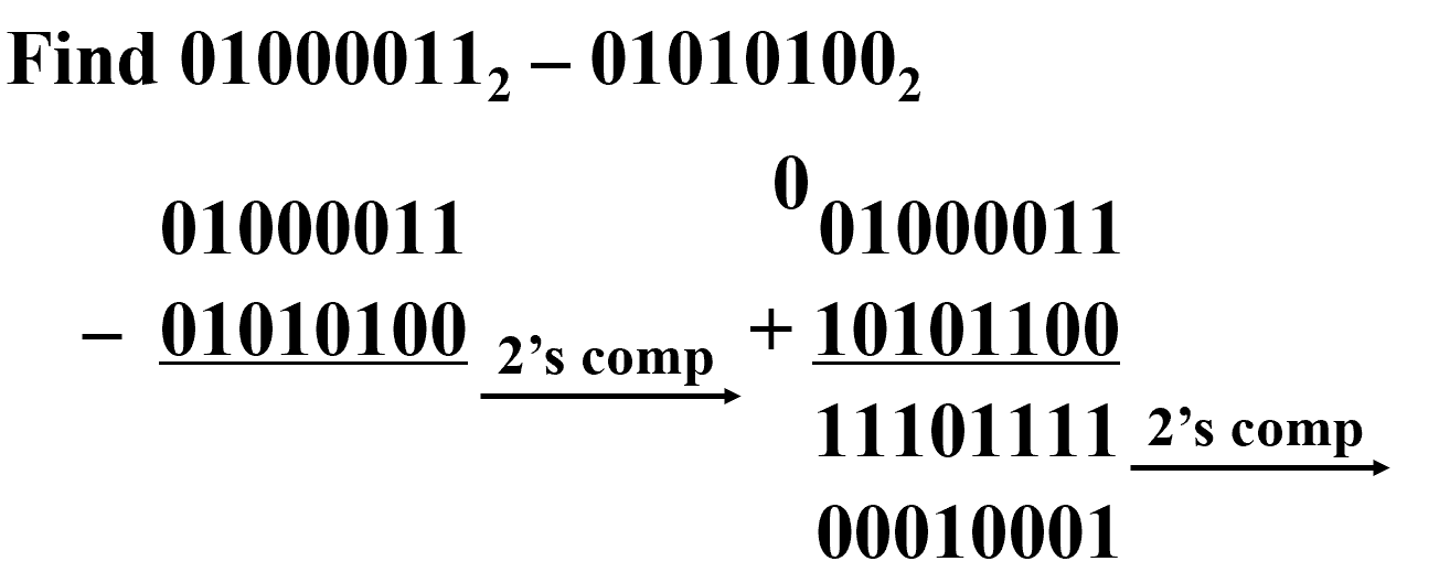
进位是 0 表明结果为负,需对结果修正
Signed Integers
- Signed Integer Representations: 第 n-1 位表示正负,后面 bits[n-2:0] 表示绝对值大小
- Signed-Complement
- Signed 1's Complement
- Signed 2's Complement
详见 ICS notes
Signed-Magnitude Arithmetic
- 检查三个符号位的奇偶性(两个操作数的符号位和加减法的符号位,我们一般认为加法是 0, 减法是 1)用于判断溢出
可能溢出的情况:正加正(000), 正减负(011), 负减正(101), 负加负(110) - If the parity of the three signs is 0:(overflow may happen)
- Add the magnitudes.
- Check for overflow (a carry out of the MSB)
- The sign of the result is the same as the sign of the first operand.
- If the parity of the three signs is 1:
- Subtract the second magnitude from the first.
- If a borrow occurs:
take the two’s complement of result and make the result sign the complement of the sign of the first operand. - Overflow will never occur.
Signed-Complement Arithmetic
- Addition:
- Add the numbers including the sign bits, discarding a carry out of the sign bits (2's Complement), or using an end-around carry (1's Complement).
- If the sign bits were the same for both numbers and the sign of the result is different, an overflow has occurred.
- The sign of the result is computed in step 1.
- Subtraction:
Form the complement of the number you are subtracting and follow the rules for addition.
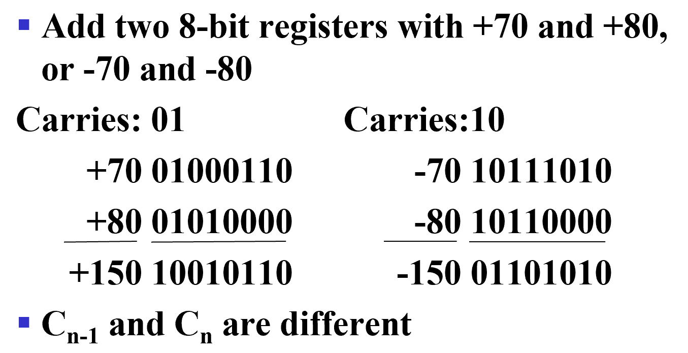
Signed 2’s Complement Examples
- 1101 + 0011
Result is 0000. The carry out of the MSB is discarded. - 1101 - 0011
Complement 0011 to 1101 and add. Result is 1010. The carry out of the MSB is discarded.
- 2’s Complement Adder/Subtractor
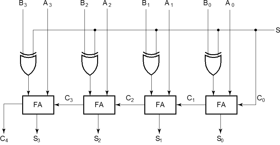
利用异或门,当 S=0 时异或门相当于保持另一个信号,当 S=1 时异或门相当于对另一个信号取反。
- Overflow Detection
Overflow occurs if n + 1 bits are required to contain the result from an n-bit addition or subtraction
Example
Simplest way to implement overflow \(V = C_n \oplus C_{n - 1}\) \(C_n\) 是溢出去的位,\(C_{n-1}\) 是运算后的符号位。 截断
Arithmetic Logic Unit (ALU)
Decompose the arithmetic circuit into:
- An n-bit parallel adder
- A block of logic that selects four choices for the B input to the adder
Example

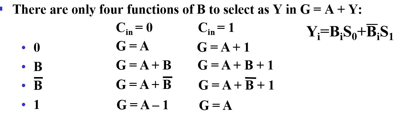
其中 \(Y_i=B_iS_0+\overline B_iS_1\)
S0 S1 的变化可以给加法器提供不同的输入,包括 -1(二进制每一位都是 1) 0 \(B\) \(\overline B\)