Combinational Logic Circuits
约 4540 个字 36 张图片 预计阅读时间 15 分钟
Abstract
-
布尔代数 (Boolean) 的概念
Boolean Algebra- 变量与真值的关系
Binary Variables - 二值逻辑和门
Binary Logic and Gates - 三种基本运算
Three basic logic operations
- 变量与真值的关系
-
基本运算法则与电路符号
Operation Definitions and Logic Gate Symbols - 基本运算公式、规则、反演,对偶规则
basic identities, DeMorgan’s Theorem, Dual Theorem - 基本逻辑电路与其逻辑特性。与,或的开、关门特点,异或的同相、反相性质
Logic Gates and implementation, AND, OR gates used to control gate open or close, XOR gates used as a controllable invertor -
逻辑函数的化简
Simplification- 化简的标准、公式化化简、最小项,最大项及其相互关系、卡诺图化简、质蕴涵项、必要质蕴涵项,门输入成本
Boolean Algebraic Proof, Boolean Function Optimization, Canonical Forms, Minterms, Maxterms and their relationship, K-map simplification, Prime Implicants, Gate input Cotes - 含任意项函数化简
Don't Cares in K-Maps
- 化简的标准、公式化化简、最小项,最大项及其相互关系、卡诺图化简、质蕴涵项、必要质蕴涵项,门输入成本
-
不同函数形式的变换及与最小项的关系
SOM form, POM form, Standard forms, SOP form, POS form, Conversion between forms - 函数的五种表示形式:真值表、逻辑解析式、波形图、卡诺图、逻辑电路图
Truth Table, Boolean Equations, Wave form, K-map, Logic Diagram - 高阻输出 ( 三态门 )
Hi-Impedance Outputs, Three state buffer
Gate Circuits and Boolen Equations
Binary Logic and Gates
Binary Logic
Binary variables take one of two values. e.g. True/False, On/Off, Yes/No, 1/0...
Logical variables operate on binary variables and binary values.
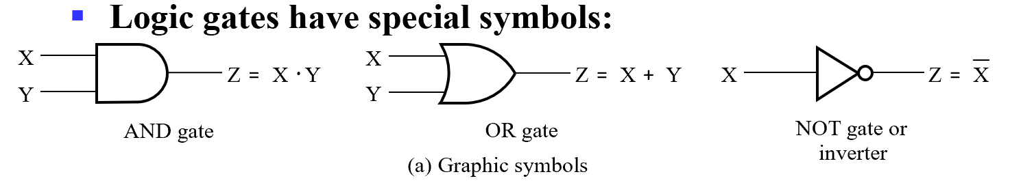
ANDdenoted by a dot(\(\cdot\) or \(\cap\))ORdenoted by a plus(+ or \(\cup\))NOTdenoted by \(\overline{a}\) ' or ~
Truth tables a tabular listing of the values of a function for all possible combinations of values on its arguments.
Logical Function Implementation:
Logical Gates
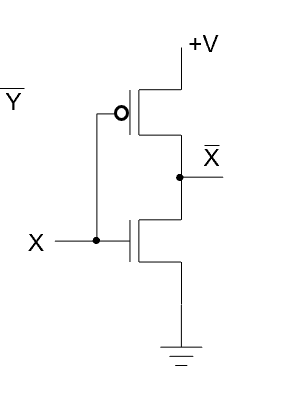
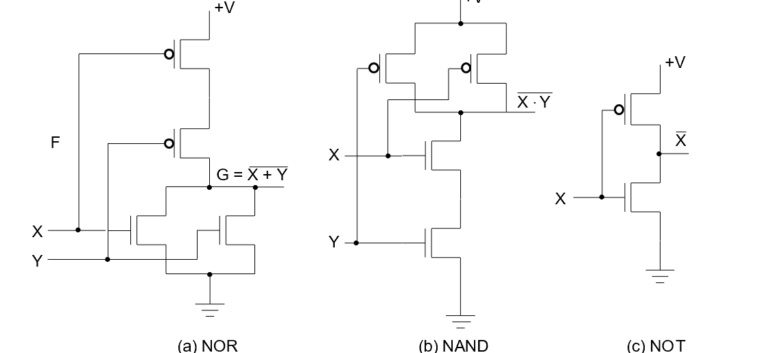
- PMOS / NMOS 上面的是 PMOS, 下面是 NMOS. PMOS 是 P 断 N 通, NMOS 是 N 断 P 通.
详见 ICS notes
NAND/NOR 才是最基本的 , 他们可以独立实现 OR AND NOT.
Question
- 能不能把两个逻辑门的输出接在一起 ?( 如 NAND 和 NOT 的输出 )?
-> 可能一个输出是 1, 一个输出是 0. 短路, 芯片烧掉, 冒烟. - 能不能把 NOT 门中变为 X 和 Y 两个输入分别对应 CMOS 和 NMOS?
->不能. 当 X,Y=1,0 时上下都接通, 短路. 当 X,Y=0,1 时输出角处于 HZ(高阻态).
三态门允许器件输出这样的结果.
Logical Gate Symbols and Behavior
waveform behavior in time:
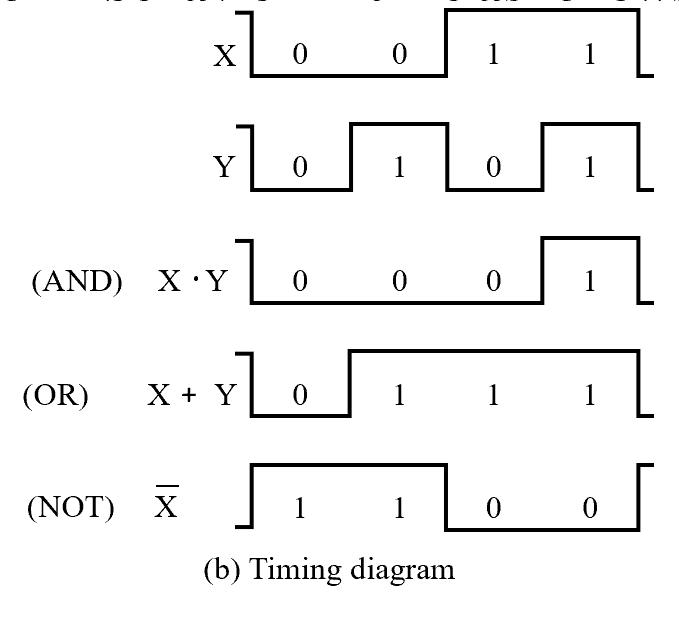
Note
注意竖向关系 . 结果在输入改变的时候改变 . 最好用直尺铅笔画出竖向虚线 .
Gate Delay
In actual physical gates, if one or more input changes causes the output to change, the output change does not occur instantaneously.
The delay between an input change(s) and the resulting output change is the gate delay denoted by tG.
很多时候我们会做 tradeoff, 使用更昂贵的器材来获得更小的 delay.
Note
只有真值表是唯一 , 确定的 . 但公式 , 原理图可以有多种形式 .
Boolen Algebra
![[ppt16]](https://s2.loli.net/2022/09/22/2q9jhpVlHw3JdWQ.png)
( 左右公式是对偶的 )
precedence: parentheses > NOT > AND > OR
The dual of an algebraic expression is obtained by interchanging + and · and interchanging 0’s and 1’s.
对偶式可以用于函数化简.
注 : 非不变 !
self-dual: the dual expression = the original expression.
Boolean Algebraic Proofs 1
AB + A'C + BC = AB + A'C (Consensus Theorem)
Justification 1: 1 . X = X
Justification 2:
X + X’ = 1
原式 = AB + A’C + ABC + A’BC X(Y + Z) = XY + XZ (Distributive Law)
= AB + ABC + A’C + A’BC X + Y = Y + X (Commutative Law)
= AB . 1 + ABC + A’C . 1 + A’C . B X . 1 = X, X . Y = Y . X (Commutative Law)
= AB (1 + C) + A’C (1 + B) X(Y + Z) = XY +XZ (Distributive Law)
= AB . 1 + A’C . 1 = AB + A’C X . 1 = X
最好将每一步用的公式写出来
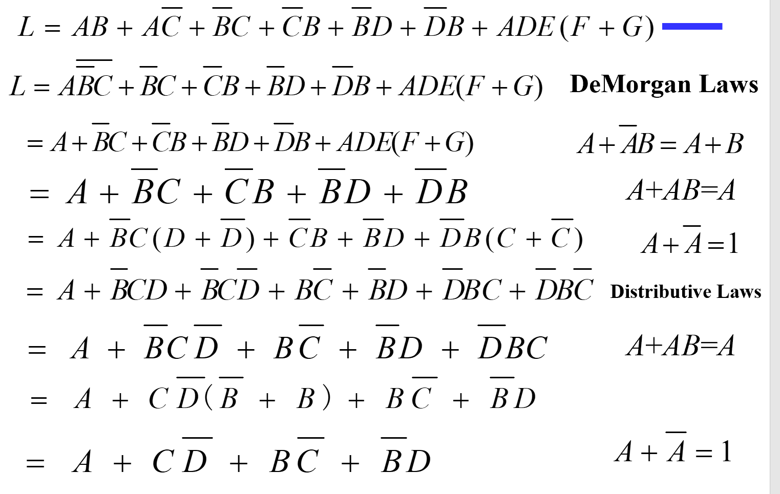
Boolean Algebraic Proofs 2
(X+Y)'Z + XY' = Y'(X+Z)
原式 = X’ Y’ Z + X Y’ (A + B)’ = A’ . B’ (DeMorgan’s Law)
= Y’ X’ Z + Y’ X A . B = B . A (Commutative Law)
= Y’ (X’ Z + X) A(B + C) = AB + AC (Distributive Law)
= Y’ (X’ + X)(Z + X) A + BC = (A + B)(A + C) (Distributive Law)
= Y’ . 1 . (Z + X) A + A’ = 1
= Y’ (X + Z) 1 . A = A, A + B = B + A (Commutative Law)
留意定理 15
Boolean Algebraic Proofs 3
Complementing Functions
Use Demorgan's Theroem
- interchange AND and OR operators.
- complement each constant value and literal.
Note
对比反函数和对偶函数 .
Canonical Forms
任何逻辑函数 , 可以写为 Sum of Minterms(SOM) or Product of Maxterms(POM).
Maxterm and Minterm
-
Minterms
Minterms are AND terms with each variable present in either true or complemented form.( 每个变量都会出现且只出现一次 )
n variables -> \(2^n\) minterms -
Maxterms
Maxterms are OR terms with each variable present in either true or complemented form.( 每个变量都会出现且只出现一次 )
n variables -> \(2^n\) maxterms
Example
| Index | Minterm | Maxterm |
|---|---|---|
| 0 | \(\overline x\ \overline y\) | \(x+y\) |
| 1 | \(\overline x\ y\) | \(x+\overline y\) |
| 2 | \(x\ \overline y\) | \(\overline x+y\) |
| 3 | \(x\ y\) | \(\overline x+\overline y\) |
The index is important for describing which variables in the terms are true and which are complemented.
index 就是对应使得 minterm = 1 的唯一的取值. e.g. index = 1 means only when x = 0, y = 1 then \(\overline{x} y = 1\)
maxterm 与 minterm 对偶, 所以 index 是使得 maxterm = 0 的唯一的取值.
如 index = 1, 则 minterm 里对应的字母应为原变量, maxterm 里的字母应为反变量.
Note that the Standard Order of variables: usually alphabetically.
We find that \(m_i = \overline{M_i}\).
-
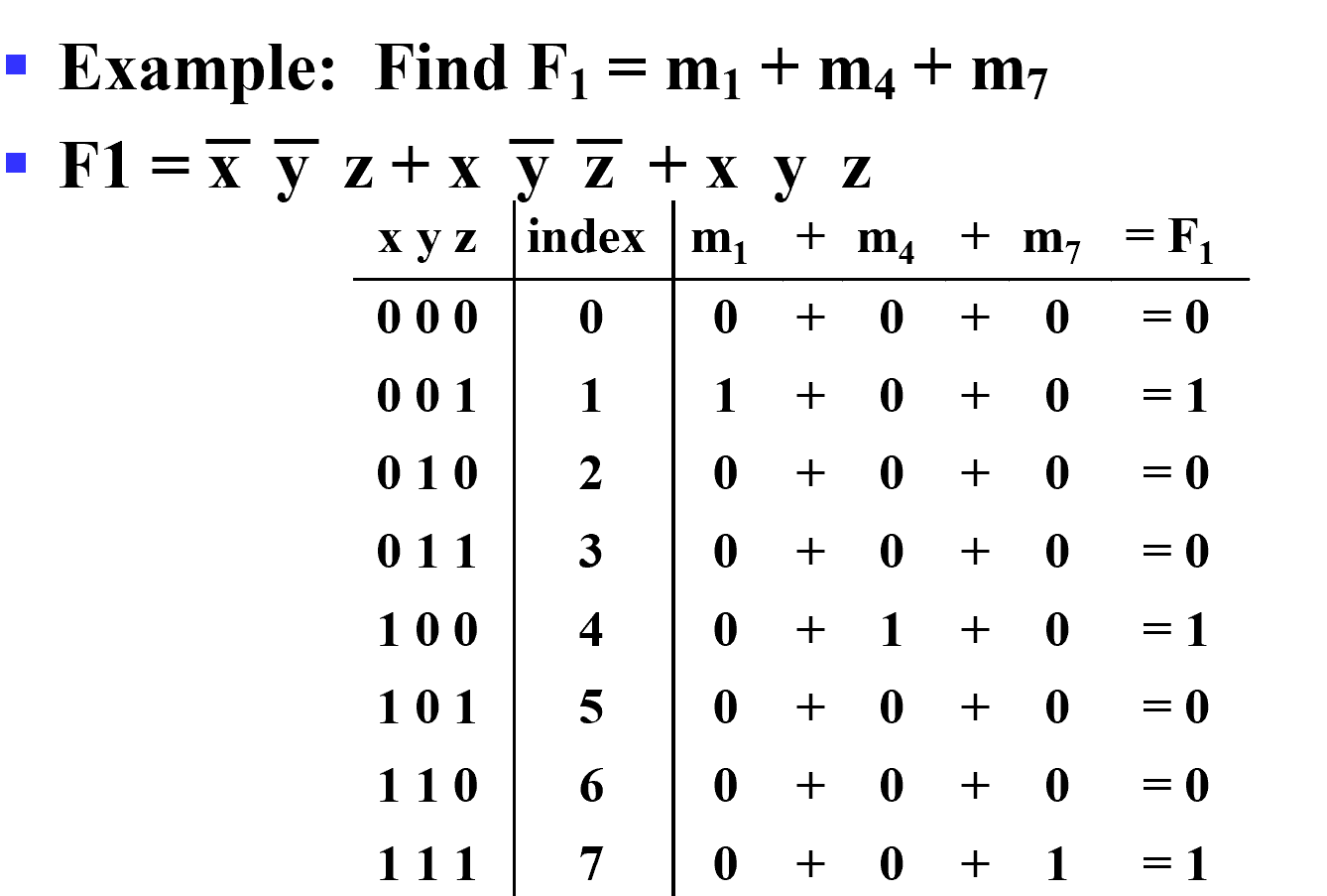
We can implement any function by "ORing" the minterms corresponding to "1" entries in the function table. These are called the minterms of the function.
Minterm Function Example
it can also be written as \(\sum m(1,4,7) = \sum(1,4,7)\).- We can implement any function by "ANDing" the maxterms corresponding to "0" entries in the function table. These are called the maxterms of the function.
Maxterm Function Example
it can also be written as \(\prod M(0, 2, 3, 5, 7) = \prod(0, 2, 3, 5, 7)\)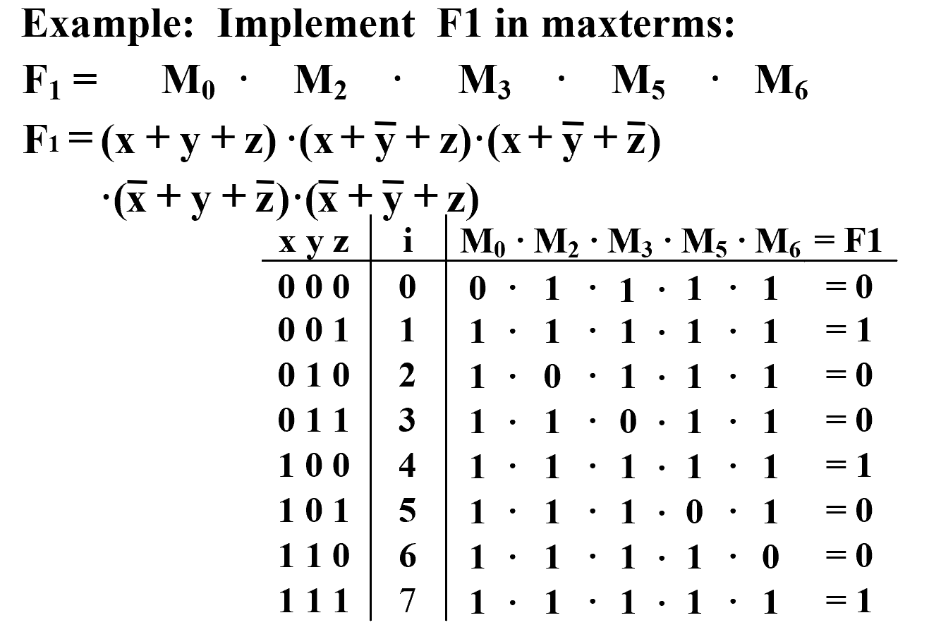
Canonical Forms
-
Canonical Sum of Minterms
Boolen function -> Sum of Minterms: expand all terms first to explicitly list all minterms. Do this by "ANDing" any term missing a variable v with a term \((v+\overline{v})\).\(F=A+\overline{B} C\)
F = A(B + B’)(C + C’) + (A + A’) B’ C
= ABC + ABC’ + AB’C + AB’C’ + AB’C + A’B’C
= ABC + ABC’ + AB’C + AB’C’ + A’B’C
= m7 + m6 + m5 + m4 + m1 = m1 + m4 + m5 + m6 + m7 -
Canonical Product of Maxterms
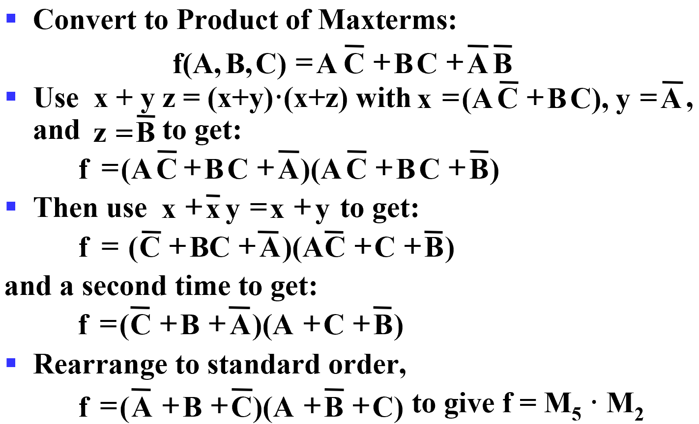
The method for Maxterms is similar, just "ORing" terms missing variables v with a term equal \(v\cdot \overline{v}\) then applying the distributive law.\(f(A,B,C)=A\overline C + BC+\overline A \overline B\)
Function Complements
The complement of a function expressed as a sum of minterms is constructed by selecting the minterms missing in the sum-of-minterms canonical forms.
每一个 minterm 要么在函数里, 要么在其反函数里. 求函数的反函数, 只需要所有minterms 去掉原函数中存在的 minterms 即可.
e.g. \(F(x,y,z)=\sum_m(1,3,5,7)\) then \(\overline F(x,y,z) = \sum_m(0,2,4,6)\)
It also can be writed as \(\overline F= \overline m_1 \cdot \overline m_3 \cdot \overline m_5 \cdot \overline m_7 = M_1 \cdot M_3 \cdot M_5 \cdot M_7=\prod _M(1,3,5,7)\)
Conversion between Forms
Idea: \(F=\sum_m m_i\) while \(\overline{F} = \sum_M M_i\)
Maxterms 的求法不是很自然, 一般先求反函数的 Minterms 再将他们取反转为 Minterms.
- Find the function complement by swapping terms in the list with terms not in the list.
- Change from products to sums, or vice versa.
如上文的例子中 \(F(x,y,z)=\sum_m(1,3,5,7), \overline{F}=\sum_m(0,2,4,6)\) 故 \(F = \prod_M(0,2,4,6)\)
Standard Forms
- Standard Sum-of-Products (SOP) form: equations are written as an OR of AND terms.
- Standard Product-of-Sums (POS) form: equations are written as an AND of OR terms
SOP and POS are two-level network of gates.
-
SOP
- The first level consists of n-input AND gates
- The second level is a single OR gate (with fewer than \(2^n\) inputs)
Info
Standard Forms 用来做电路实现, 一般会进行 SOM POM 化简 , 但会省略一些东西 . 依然按照 Standard Order, 但每一项中不一定需要所有变量 .
SOP POS 也被称为两极函数.
如 SOP: \(ABD+\overline A \overline B C +B\), POS: \((A+B)\cdot (A+\overline B+\overline C)\cdot C\) 他们路径上最多只需要经过两个电路门 , 这称为二级电路 .
反观 \((AB+C)(A+C), AB\overline C+AC(A+B)\) 最多就需要经过三个电路门.
- 为什么需要降低电路门的级数 ?
电路门有延迟, 经过的电路门越多延迟越大, 意味着最后电路做出来的计算机不易提高功率.
\(F = \overline A\overline B C + A \overline B\overline C + A\overline B C + AB\overline C + ABC\)
F = A’ B’ C + A (B’ C’ + B C’ + B’ C + B C)
= A’ B’ C + A (B’ + B) (C’ + C)
= A’ B’ C + A.1.1
= A’ B’ C + A
= B’C + A
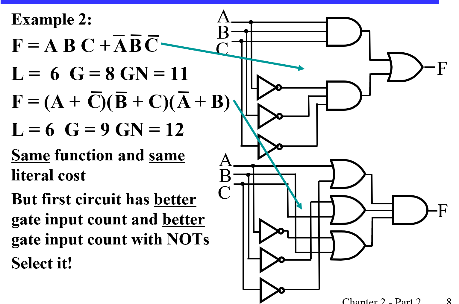
Circuit Optimization
Goal: To obtain the simplest implementation for a given function.
Distinct cost criteria we will use:
- Literal cost (L)
- Gate input cost (G)
- Gate input cost with NOTs (GN)
Two-Level Optimization
Literal Cost
literal is a variable or its complement literal cost is the number of literal appearances in a Boolean expression corresponding to the logic circuit diagram.
e.g.
- \(F=BD+A\overline BC+ A\overline C\overline D\) its L=8
- \(F=BD+A\overline BC+ A\overline B\overline D + AB\overline C\) its L=11
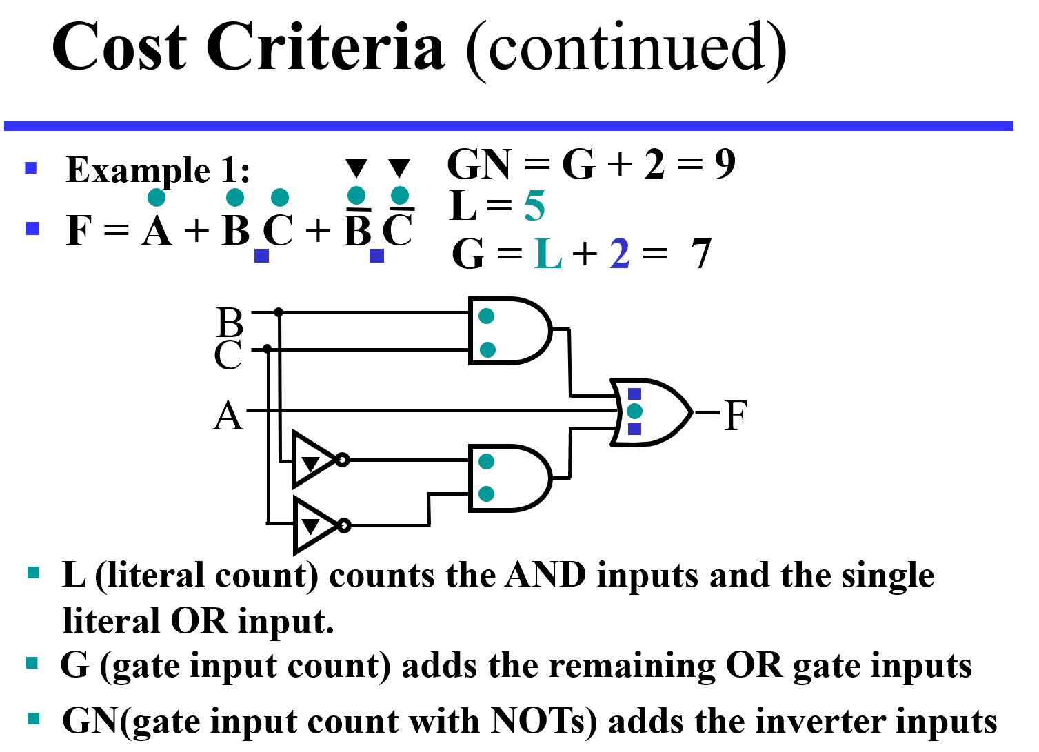
Gate Input Cost
Gate input costs is the number of inputs to the gates in the implementation corresponding exactly to the given equation or equations. (G - inverters not counted, GN - inverters counted)
For SOP and POS equations:
- all literal appearances(L)
- the number of terms excluding single literal terms, (G).
e.g. for A+BC its L=3 while G=1 - optionally, the number of distinct complemented single literals(GN).
e.g.
- \(F=BD +A\overline BC+A\overline C\overline D\) G=8(L)+3=11, GN=11+3=14.
- \(F=BD+A\overline BC+A\overline B\overline D+AB\overline C\) G=11+4=15, GN=15+3(only BCD)=18.
Cost Criteria
When do we stop trying to reduce the cost?
Do we know when we have a minimum cost?
Map Manipulation
Karnaugh maps(K-map)
- A K-map is a collection of squares Each square represents a minterm
- The collection of squares is a graphical representation of a Boolean function
- Adjacent squares differ in the value of one variable
- Alternative algebraic expressions for the same function are derived by recognizing patterns of squares
The K-map can be viewed as
- A reorganized version of the truth table
- A topologically-warped Venn diagram as used to visualize sets in algebra of sets
Two-Variable Maps
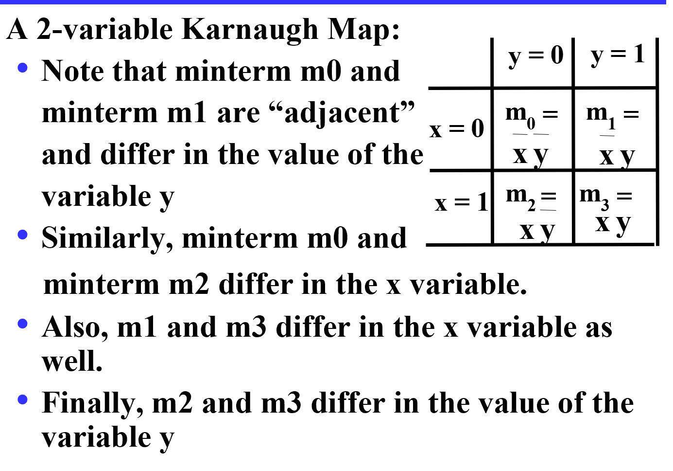
Example
| F=x+y | y=0 | y=1 |
|---|---|---|
| x=0 | 0 | 1 |
| x=1 | 1 | 1 |
For function F(x,y), the two adjacent cells containing 1’s can be combined using the Minimization Theorem:
\(F(x,y)=(x \ \overline y + x\ y ) + (x\ y + \overline x \ y) = x + y\)
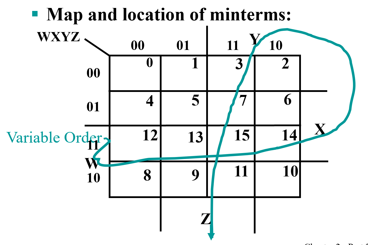
Three-Variable Maps
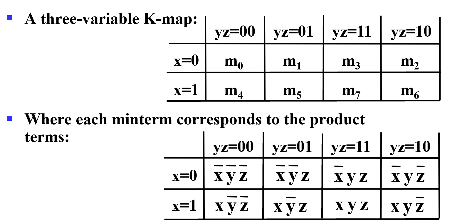
Note
注意列 , 要按照 Gray codes 的顺序排列 , 即相邻两列只相差一位 . 因此列标号为 00 01 11 10.
相邻两个小方格都只有一个变量不同.
可以卷起来, 即最左边一列和最右边一列
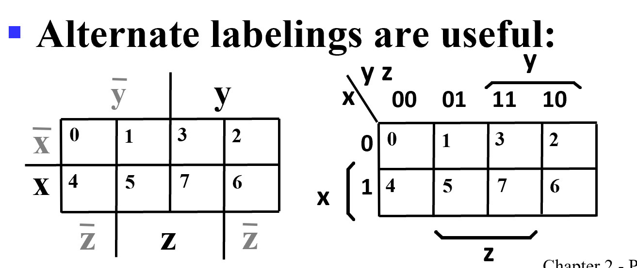
Alternatie Map Labeling
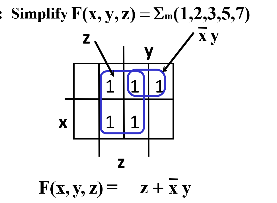
Example
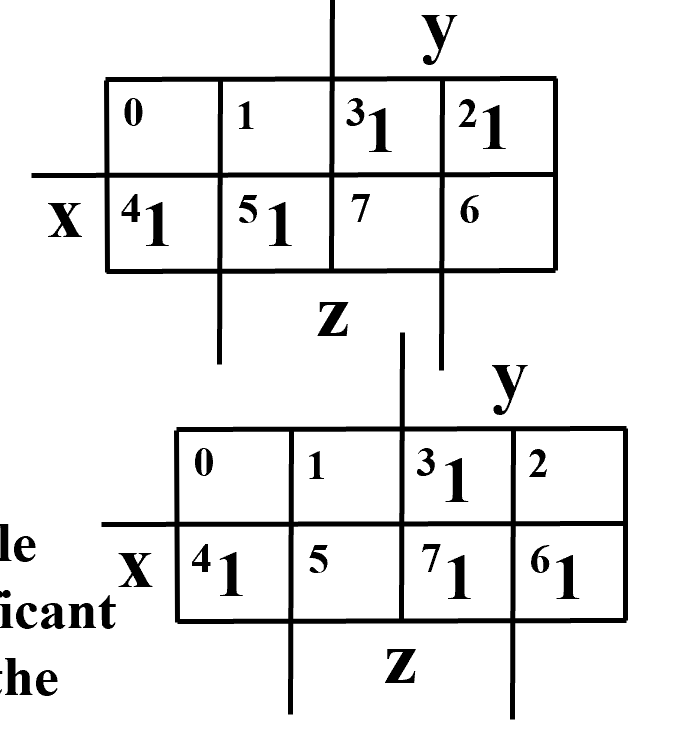
- 注意到 3 2 格都是 1, 因此 \(\bar xy\bar z + \bar x y z = \bar xy\), 没有变化的变量可以保留 , 变化了的变量可以消掉 . 同理 4 5 格可化为 \(x \bar y\)
- 3 7 格 : \(yz\); 6 7 格 : \(x y\); 4 6 格 \(: x\bar z\)
Combining Squares
可以画 \(2^n\) 大小的方形格 ( 即一次要包括 \(2^n\) 个小方格 )
For 3-variable K-Map:
- One square represents a minterm with three variables
- Two adjacent squares represent a product term with two variables
- Four “adjacent” terms represent a product term with one variable
- Eight “adjacent” terms is the function of all ones (no variables) = 1.
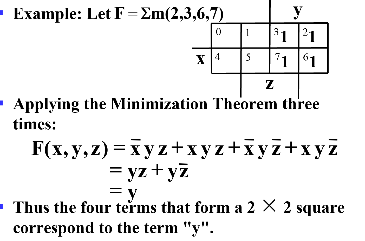
Example
Warning
- 格雷码 !
- 两侧可以卷起来
化简思路 : 用最大的最少的圈把所有的 1 圈完 .( 圈与圈之间可以有交叉 )
一定是 SOP
Example
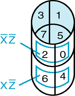
Four Variable Maps
Note
注意四个角也可以卷 (0 2 8 10 -> \(\overline X \ \overline Z\))
Example
化简结果不唯一
Don't Cares( 无关项 ) in K-Maps
By placing “don't cares” (an “x” entry) in the function table or map, the cost of the logic circuit may be lowered.
如我们把 BCD 码作为输入, 有效数字 0 - 9, 如果那么 9 以上的输入组合我们不在乎输出结果, 称为无关项, 在卡诺图上画 x.
BCD 5 or More
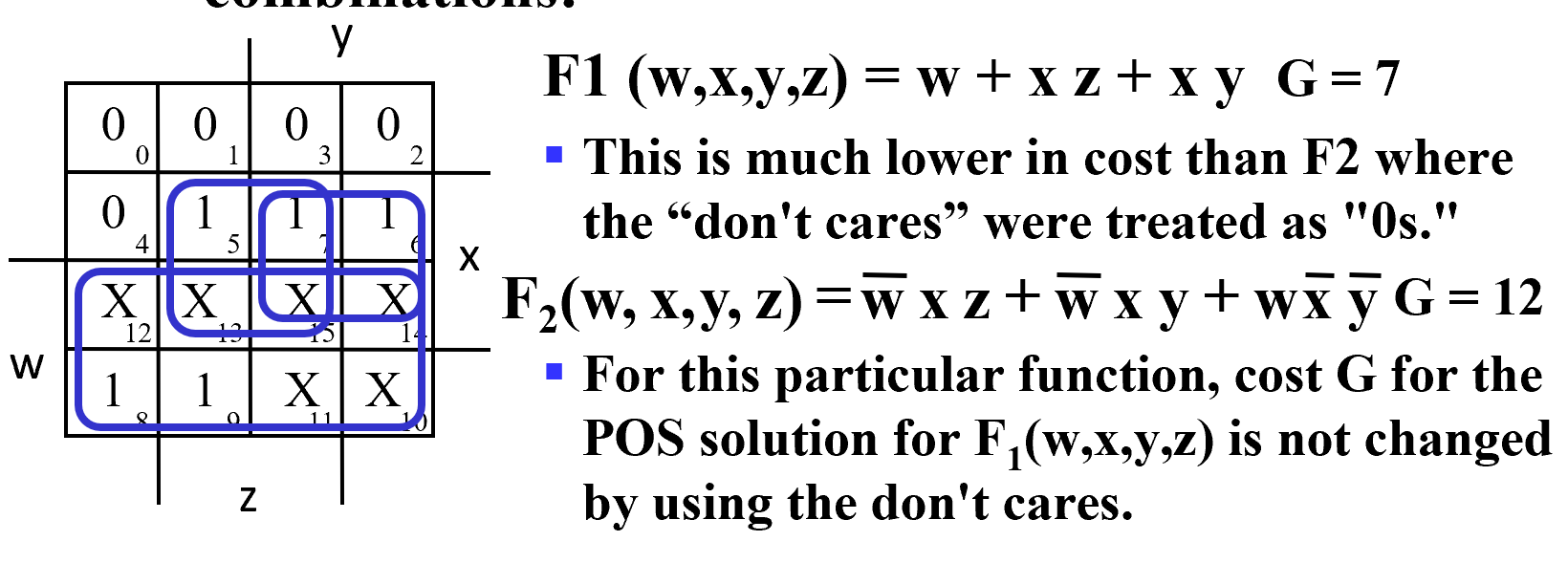
X 可圈可不圈!
Example
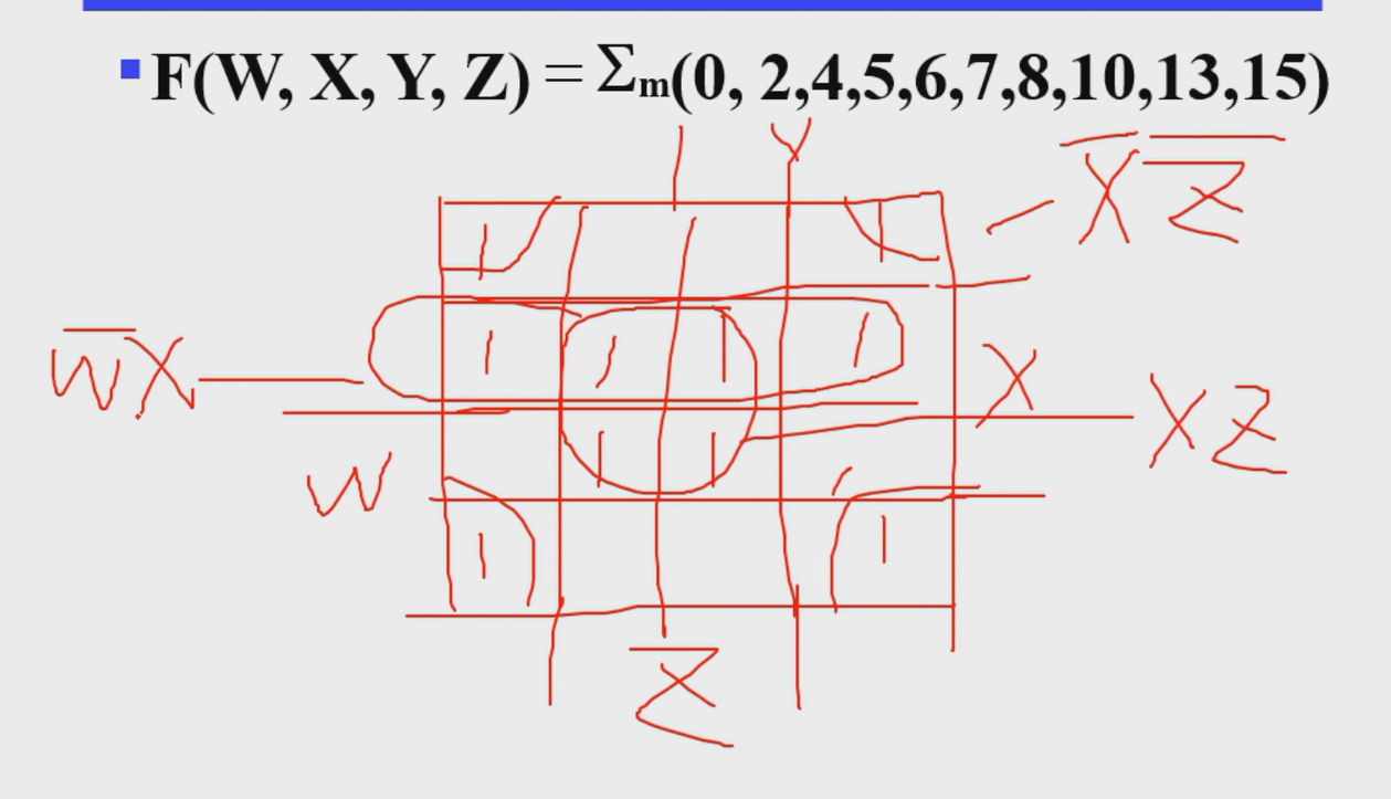
Find the optimum POS solution: \(F(A,B,C,D)=\sum\limits_m(3,9,11,12,13,14,15)+\sum d(1,4,6)\)
Hint: Use \(\overline F\) and complement it to get the result.
ans:
F' = B' D' + A' B (求 F' 时在卡诺图中圈空格,而不是 1)
F = (B + D)(A + B')
Systematic Simplification
- A Prime Implicant( 质蕴含项 ) is a product term obtained by combining the maximum possible number of adjacent squares in the map into a rectangle with the number of squares a power of 2.
- A prime implicant is called an Essential Prime Implicant( 必要质蕴涵项 ) if it is the only prime implicant that covers (includes) one or more minterms.
质蕴涵项是对某个 "1" 而言包括它的最大方形。对某个 "1" 而言如果它的质蕴涵项只有一个,那么它是必要的。
- Find All Prime Implicants
- Find Essential ones
- 处理剩下的 1
Example
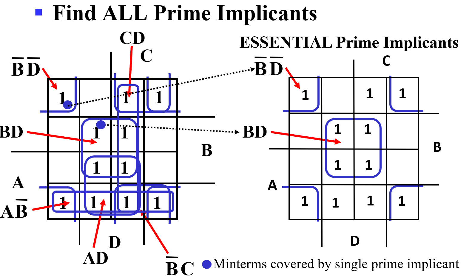
哪些 1 只被一个质蕴含圈包围,那么他一定是必要质蕴涵项
Example
Find all prime implicants for:
\(G(A,B,C,D)=\sum\limits_m(0,2,3,4,7,12,13,14,15)\)
Hint: There are seven prime implicants!
Prime Implicants are AB, B C' D', A' C' D', A' B' D', A' B' C, A' C D, B C D. ony AB Essential.
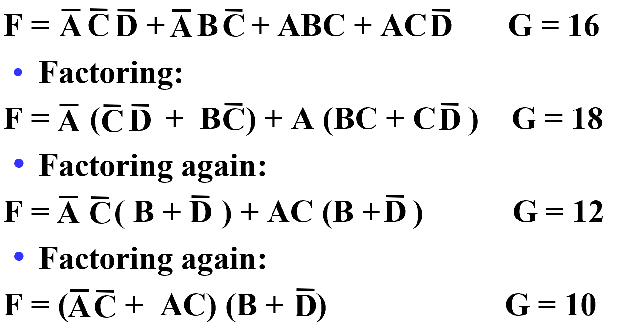
Multi-Level Circuit Optimization
两级门的延迟低,但 cost 高。
Transformation Examples
Integrated Circuits
集成电路
- Integrated circuit (informally, a “chip”) is a semiconductor crystal (most often silicon) containing the electronic components for the digital gates and storage elements which are interconnected on the chip.
-
Terminology - Levels of chip integration
- SSI (small-scale integrated) - fewer than 10 gates
- MSI (medium-scale integrated) - 10 to 100 gates
- LSI (large-scale integrated) - 100 to thousands of gates
- VLSI (very large-scale integrated) - thousands to 100s of millions of gates
-
Technology Parameters
- Fan-in 扇入系数 – the number of inputs available on a gate
一个门的输入端的上限
理想情况一个门的输入可以接无数个门的输入,但实际上因为每一个门的输入端都会花费一些电流,而门输出的电流是有限的,从集成电路本身会要求一个门的输出最多能拉多少门的输入。 -
Fan-out 扇出系数 – the number of standard loads driven by a gate output
一个门的输出带了很多门的输入?(像火车头带了很多车厢)
一个门的输出不能接到太多门的输入上去,一般会用 buffer 做缓冲- e.g. 1 standard load equals the load contributed by the input of 1 inverter.
- Transition time - the time required for the gate output to change from H to L, \(t_{HL}\), or from L to H, \(t_{LH}\)
带的门越多,上升时间就越多。 我们会限制过渡时间,设置 maximum fan-out- Logic Levels – the signal value ranges for 1 and 0 on the inputs and 1 and 0 on the outputs (see Figure 1-1)
- Noise Margin – the maximum external noise voltage superimposed on a normal input value that will not cause an undesirable change in the circuit output
- Cost for a gate - a measure of the contribution by the gate to the cost of the integrated circuit
Ignoring the wiring area, the gate area is roughly proportional to the gate input count. - Propagation Delay – The time required for a change in the value of a signal to propagate from an input to an output
- Power Dissipation – the amount of power drawn from the power supply and consumed by the gate
- Fan-in 扇入系数 – the number of inputs available on a gate
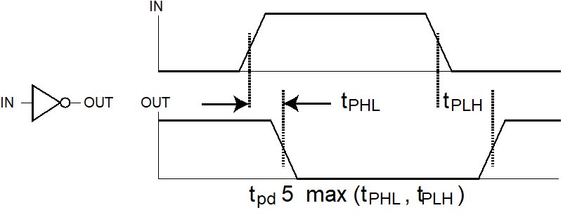
Propagation Delay
Delay is usually measured at the 50% point with respect to the H and L output voltage levels.
High-to-low (\(t_{PHL}\)) and low-to-high (\(t_{PLH}\)) output signal changes may have different propagation delays.
注意 HL/PL 指的是输出端的时间变化。
Info
如果这里有 n 个非门串联
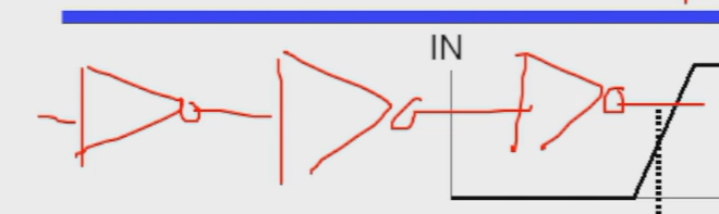
计算 \(t_{PHL}\) 需要 \(t_{3PHL} + t_{2PLH} + t_{1PHL}\)
从结果倒推
如果只求 \(t_{pd}\) 只需要把每级的 \(t_{pd}\) 相加即可。
-
Delay Mode
- Transport delay - a change in the output in response to a change on the inputs occurs after a fixed specified delay
输出整体往后移 -
Inertial delay - similar to transport delay, except that if the input changes such that the output is to change twice in a time interval less than the rejection time, the output changes do not occur. Models typical electronic circuit behavior, namely, rejects narrow “pulses” on the outputs 除了输出往后移,在惯性延迟下,很窄的脉冲(小于 rejection time)会被消除掉。
Example

蓝线表明 propagation time, 黑线表明 rejection time.
因此 ab de 这个脉冲被吃掉
- Transport delay - a change in the output in response to a change on the inputs occurs after a fixed specified delay
-
Circuit Delay
Example
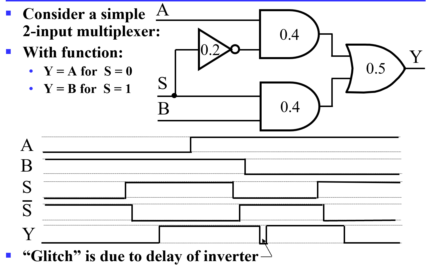
- 最开始 S 由 0->1 后 0.9s Y 从 0->1
- S 从 1->0 后下方的与门 0.4s 后会从 1->0, 但上方的与门 0.6s 后才会从 0->1. 但 0.9s 后 Y 才会 1->0, 此后再过 0.2s( 共 1.1s) 后 Y 从 0-> 1.
这里 Y 出现了一个小尖峰,我们称之为电路产生的冒险。
S 的两条路径我们发现延迟不同,这种我们称之为电路中的竞争。
-
Fan-out and Delay
The fan-out loading a gate’s output affects the gate’s propagation delay。
SL(Standard Load): 以非门为标准。带一个非门需要 ... 的负载Example
One realistic equation for tpd for a NAND gate with 4 inputs is: \(t_{pd} = 0.07 + 0.021 SL\) ns SL is the number of standard loads the gate is driving, i. e., its fan-out in standard loads For SL = 4.5, tpd = 0.165 ns
由工艺程度+负载情况决定 -
Cost/Performance Tradeoffs
Example
NAND gate G with 20 standard loads on its output has a delay of 0.45 ns and has a normalized cost of 2.0.
A buffer H has a normalized cost of 1.5. The NAND gate driving the buffer with 20 standard loads gives a total delay of 0.33 ns
1. The cost of this portion of the circuit cannot be more than 2.5 2. The delay of this portion of the circuit cannot be more than 0.40 ns 3. The delay of this portion of the circuit must be less than 0.40 ns and the cost less than 3.0ans: 1. No buffer
2. Use buffer
3. Irrelevant - buffer needed to satisfy delay constraint, but cannot satisfy cost constraint.
Additional Gates and Circuits
Other Gate Types
Why?
- Implementation feasibility and low cost
- Power in implementing Boolean functions
- Convenient conceptual representation
Gate classifications
- Primitive gate - a gate that can be described using a single primitive operation type (AND or OR) plus an optional inversion(s).
- Complex gate - a gate that requires more than one primitive operation type for its description
Primitive gate
Buffer
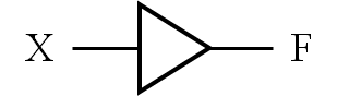
没有逻辑功能,但有很强的带负载的能力,能够拉高电平,降低传输延迟。
NAND
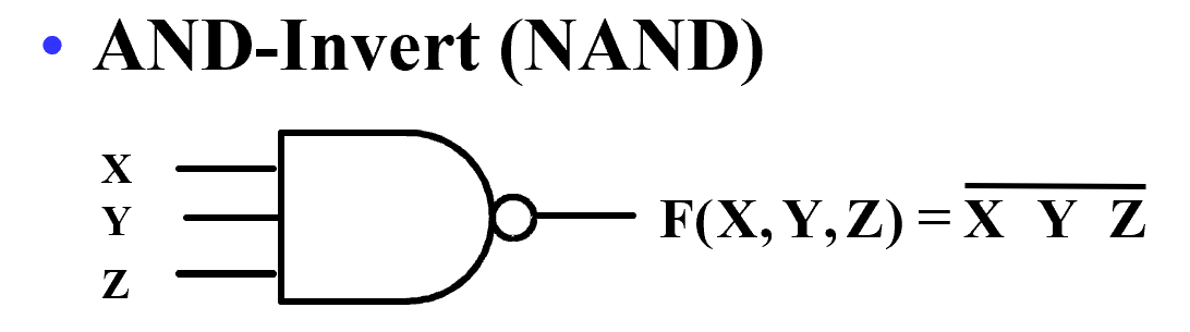
与非也可以认为是先非后或 \(F=\overline{X} + \overline{Y} + \overline{Z}\)
A NAND gate with one input degenerates to an inverter.
Universal gate - a gate type that can implement any Boolean function.
最高效
我们一般不使用与非门做逻辑运算,因为他不满足交换、结合律。一般在最后把与或非转为用与非实现。
NOR
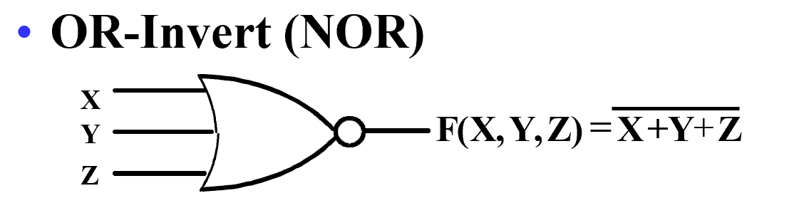
也可以利用 De Morgan 变为 先非后与,其他同与非。
Complex gate
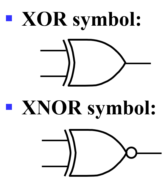
Exclusive OR/ Exclusive NOR
eXclusive OR(XOR) and XNORs gate
-
Definitions:
- \(X\oplus Y = X\ \overline Y +\overline X \ Y\)
- \(\overline{X\oplus Y} = X\ Y +\overline X \ \overline Y\)
- the XNOR function also known as the equivalence function, denoted by the operator '\(\equiv\)'.
- 重要公式(要记)
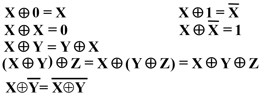 ( 第一行 & 最后一行很重要 )
-
严格来说,只有两变量的异或。对于多于两个输入的,我们用奇函数 / 偶函数代替。
对于三变量的异或 \(X\oplus Y\oplus Z = \overline X \ \overline Y \ Z + \overline X \ Y \overline Z + X \ \overline Y \ \overline Z + X\ Y\ Z\) 卡诺图无法再化简1 1 1 1 我们称它为奇函数,因为 minterm 里 1 的个数 (\(=\sum m(1(001),2(010),4(100),7(111))\)) 为奇数。其反函数为偶函数。
-
Symbol
注意 bubble 泡泡(表示 inverter)
- Implementation
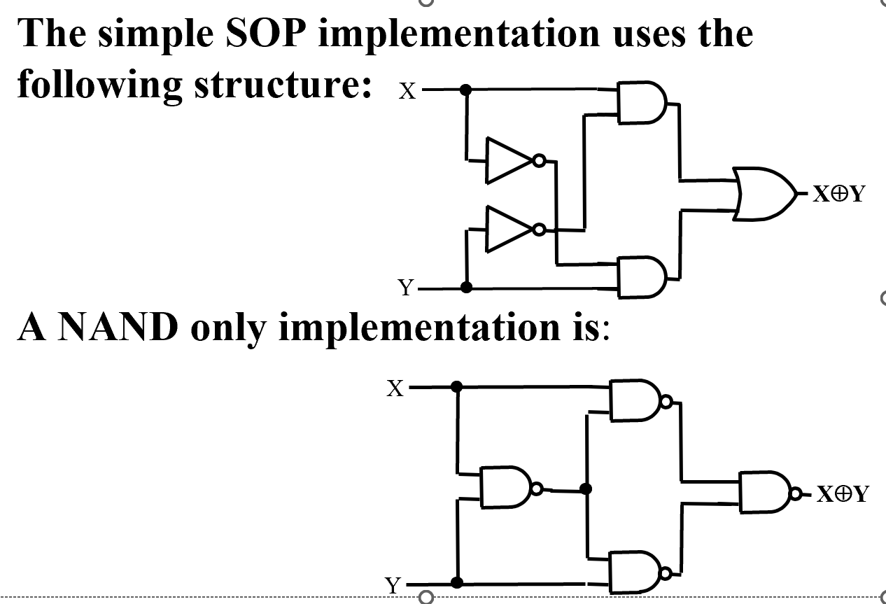
下面的实现需要 \(4\times 4=16\) 个晶体管。但实际中最简单只需要 10 个晶体管,就可以构造出 XOR 门。
Odd and Even Functions
- The 1s of an odd function correspond to minterms having an index with an odd number of 1s.
- The 1s of an even function correspond to minterms having an index with an even number of 1s.
Example
xor 都是奇函数 .
如 \(F=(X\oplus Y)\oplus Z \\ F=(W\oplus X)\oplus (Y\oplus Z)\)
-
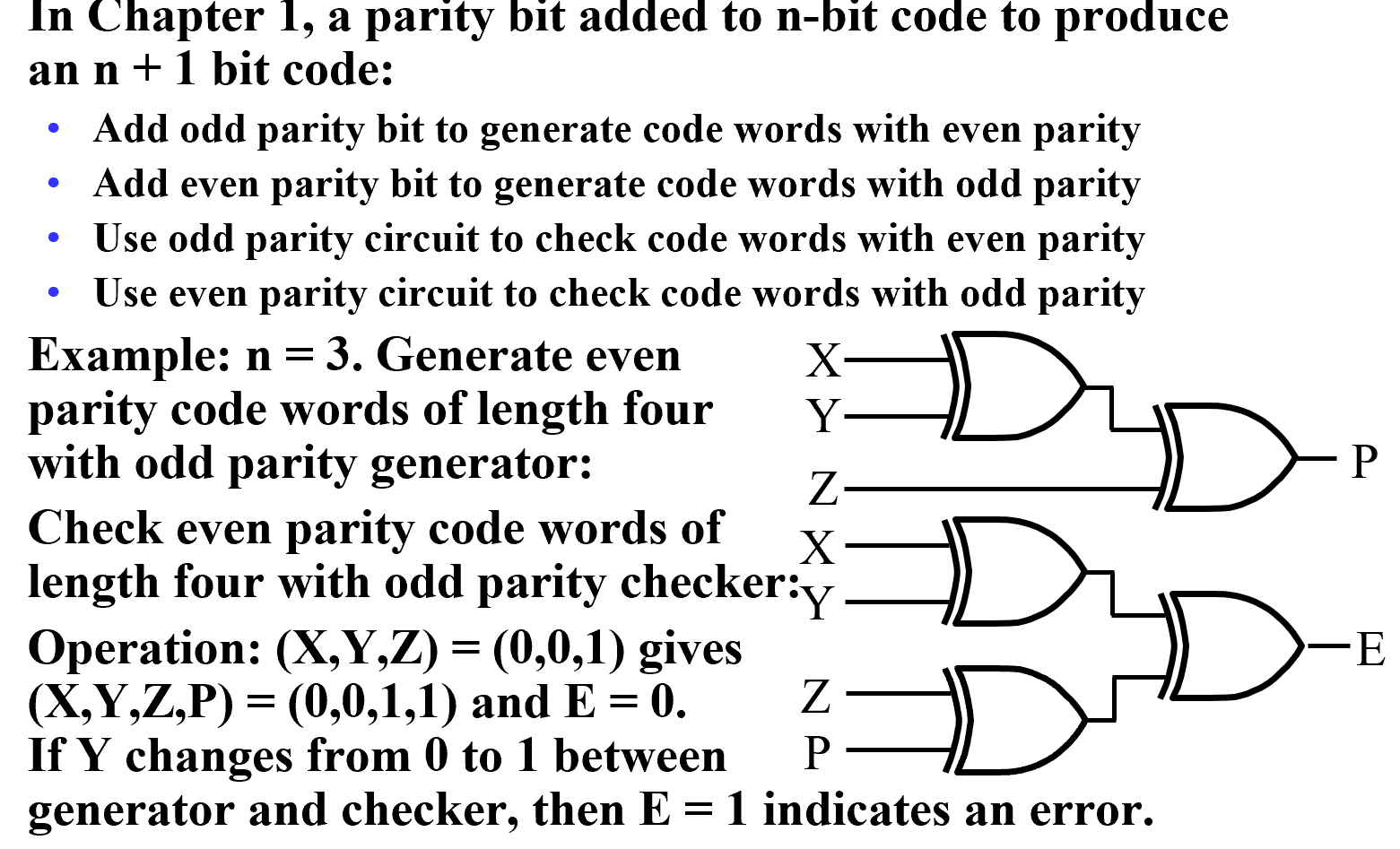
Parity Generators and Checkers 奇偶校验:传输若干个数据位,增加一个数据位,用来表示数据位的奇偶性。输入和输出端的奇偶位应该相同。
Example
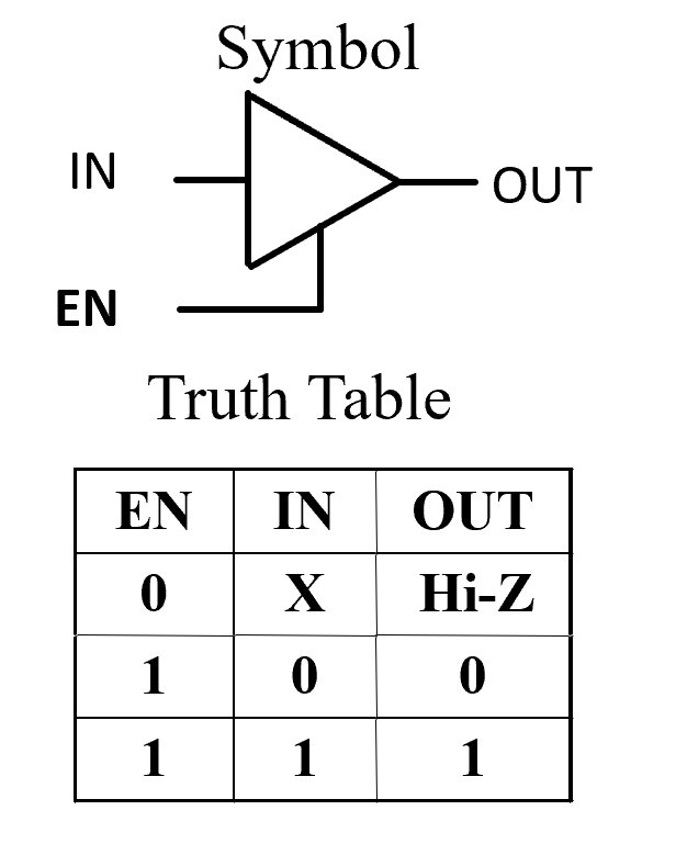
Hi-Impedance Outputs
高阻输出
Three-state logic adds a third logic value, Hi-Impedance (Hi-Z), giving three states: 0, 1, and Hi-Z on the outputs.
有条件情况下允许门的输出接在一起。
- 3-State Buffer
- Resolving 3-State Values on a Connection
把两个三态门的输出接在一起:
Resolution Table
| B1 | B0 | OUT |
|---|---|---|
| 0 | Hi-Z | 0 |
| 1 | Hi-Z | 1 |
| Hi-Z | 0 | 0 |
| Hi-Z | 1 | 1 |
| Hi-Z | Hi-Z | Hi-Z |
Info
不允许同时两个门同时输出有效输出!否则可能产生大电流损坏电路。
因此对于 n 个三态门,共 2n+1 种有效组合。
- 3-State Logic Circuit
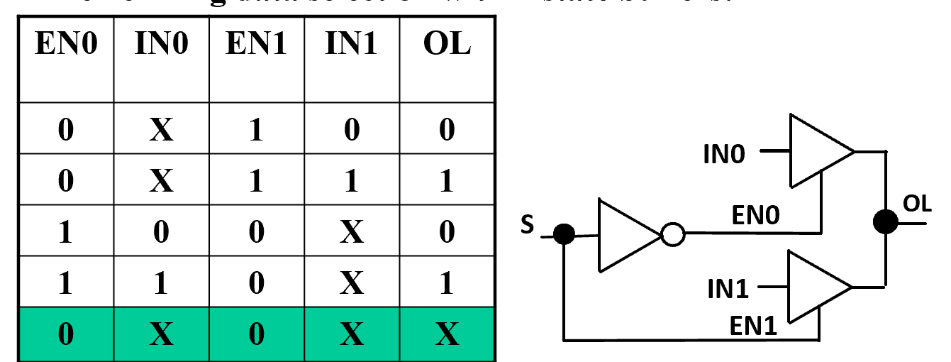 此时,两个三态门不会同时输出有效输出。
More Complex Gates
The remaining complex gates are SOP or POS structures with and without an output inverter.
- A - AND
- O - OR
- I - Inverter Numbers of inputs on first-level “gates” or directly to second-level “gates”
e.g. AOI(AND-OR-Invert), 2-2-1 AO means 2-input ANDS driving an OR with one additional OR input.