Chapter 4 The von Neumann Model
约 1259 个字 6 张图片 预计阅读时间 4 分钟
Abstract
Covered in Lecture 3, 2022.7.13 and Lecture 4, 2022.7.14
Topics:
1. The von Neumann Model
2. Brief introduction to the instruction in LC-3
Basic Components

An important idea missing in Chapter 1: All computers containing the five parts are capable of computing exactly the same things given enough time and enough memory. The only difference is the time and memory.
Note that CPU = Control and Processing Unit.
Abstract
PC 指向要执行的命令 ( 地址 ), IP 存储当前执行的命令 .
Control Unit 向 Processing Unit 发出信号(如执行加法).
Processing Unit 负责执行命令, 其中 TEMP 为寄存器, 速度相比从内存中读取数据快很多(因为内存属于 CPU 外的事物)
Memory
Memory is used to store information. Every memory location has an address asscoiated, and store a value in that location.
| Address | Stored Value |
|---|---|
| 0 | .. |
| 1 | .. |
| 2 | 4 |
| 3 | .. |
| 4 | 2 |
location 2 is called pointer variable.
Address Space and Addressability
just for review.
- Address space: The number of uniquely identifiable memory locations.
- Addressability: The number of bits stored in each memory location.
Read from the memory
- Load the address you want read to MAR(Memory's Address Register), then interrogate the memory.
- The information stored in the location having that address will be placed in the MDR(Memory's Data Register).(automatically?)
Write to the memory
- Load the address you want write to MAR, and the value to be stored in the MDR, then interrogate the memory.
- The information contained in the MDR will be written into the memory location whose address is in the MAR.
Processing Unit
Processing unit is the actual unit that carries out the processing of information in the computer.
Processing unit can be complex, but now we only focus on the simple case.
ALU(Arithmetic and Logic Unit)
ALU normally proccess data element of a fixed size referred to as the word length of the computer. The data elements are called words.
In LC-3, ALU can perform ADD, AND and NOT operations. And it process 16-bits words, which means it has a word length of 16 bits.
TEMP
usually refer to register to store information temporarily.
Why we need register?
内存不属于 CPU, 因此从中读取数据会很慢 .
因此我们一般使用寄存器来暂时存储数据, 以便运算.
Typically, the size of each register is identical to the size of values processed by the ALU.
In LC-3, we have 8 registers(R0, R1, ... R7), each containing 16 bits.
Input and Output
Some devices that get input from users, and some display the result to users.
Control unit
It is in charge of making all the other parts of the computer play together. When we describe the step-by-step process of executing a computer program, it is the control unit that keeps track of both where we are within the process of executing the program and where we are in the process of executing each instruction. Control unit in LC-3 consists of program counter(PC) and instruction register (IR). PC contains the address of the next instruction, IR contains the current instruction.
Instruction Processing
- Operation instructions: operate on date. e.g. ADD, AND, NOT
- data movement: move information from the processing unit to and from memory and to and from input/output devices. e.g. load, store
- control: altering the sequential processing of instructions. e.g. BR
The Instruction
ADD
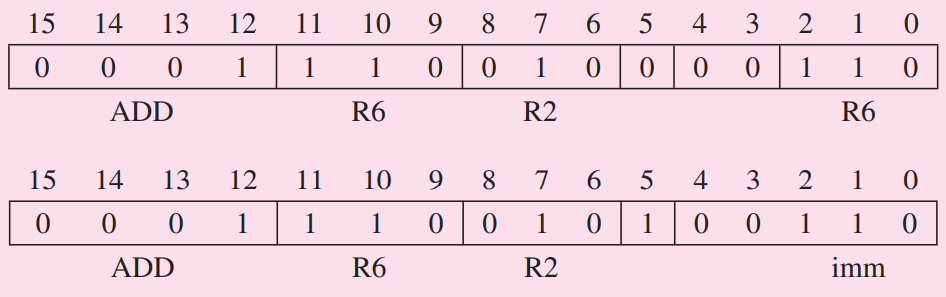
reg + imm5 -> reg / reg + reg -> reg
- bits[15:12]: opcode, 0001<->ADD
- bits[11:9]: DR(Destination Register)
- bits[8:6]: SR1(Source Register 1)
-
bits[5]:
-
bits[5]=0, the form is
SR1 + SR2 -> DRthen bits[5:3] is just used to fill the space. bits[3:0]: SR2 - bits[5]=1, then form is
SR1 + imm5 -> DRthen bits[5:0] will be sign-extended to 16 bits as the second operand.
AND
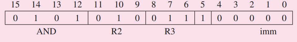
reg AND imm5 -> reg / reg AND reg -> reg (the same as ADD except the opcode 0101)
Trick
We can set bit[5]=1 and set bit[4:0]=0, and let SR1=DR.
Then the instruction becomes Reg AND 0 -> Reg, we refer to this technique as initializeing reg to 0.
LD
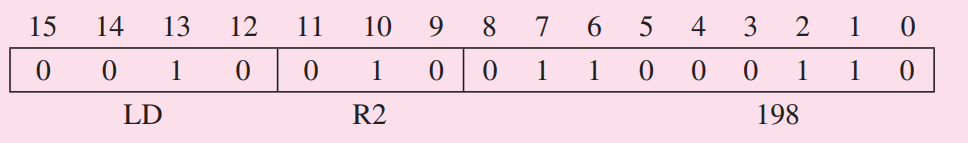
LD represent load, which means go to a particular memory location, read the value and store it in one of the registers.
LD takes PC+offset as its addressing mode, which we will introduce in detail later.
- bits[15:12]: opcode, 0010<->LD
- bits[11:9]: DR, stored the value that will be read from the memory.
- bits[8:0]: offset, and it also will be sign-extended to 16 bits. Then PC+offset will be the source address. Eventually,
M[PC+offset] -> DR.
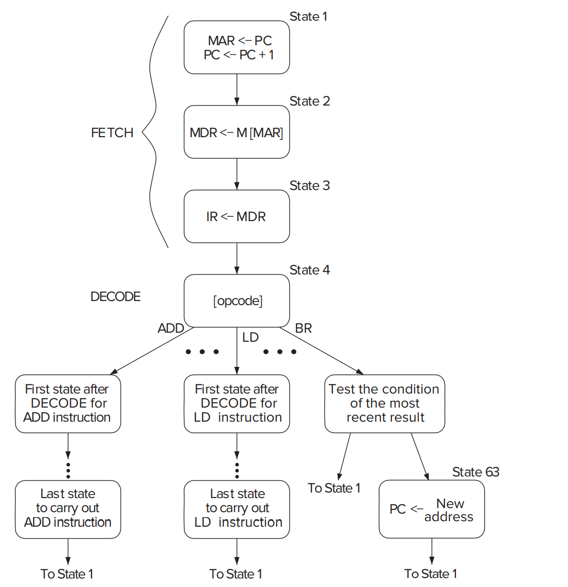
The Instruction Cycle
Instructions are processed under the direction of the control unit in a very systematic, step-by-step manner. It consists of 6 sequential phases.
Note that the instruction cycle is not the clock cycle rather made up by it and not all instructions need all 6 phases.
Fetch
Obtain the next instruction from memory and load it into IR.(Instruction Register)
IP!=IR
IP(Instruction Pointer) is a pointer to the the instruction while IR is the value of the instruction(contain opcode, register bits and sth).
IP->IR(IP = the address of IR)
- Load the MAR with the contents of the PC, and simultaneously increment the PC. (in one clock cycle)
- Interrogate memory, resulting in the instructio being placed int the MDR. (in at least one clock cycle)
- Load the IR with the contents of the MDR. (in one clock cycle)
Decode
Examine the instruction in order to figure out what the microarchitecture is being asked to do.(by decoders)
In LC-3, IR[15:12] will be decoded.
Evaluate address
Computes the address of the memory location that is needed to process the instruction, and this phase only happens when we go to memory to specify where we will store in or where we will read from. e.g. LD has this phase.
Fetch Operand
Obtain the source operands needed to process the instruction. e.g. In the LD example, loading MAR with the address calculated in the EVALUATE ADDRESS phase and reading that memory that resulted in the source operand being placed in MDR.
Execute
Carries out the execution of the instruction. e.g. add two values.
Store Result
Writes the result to its designated destinations.
ADD in LC-3
An ADD instruction can fetch its source operands, perform the ADD in ALU and store the result all in a single clock cycle.
Changing the Sequence of Execution
BR
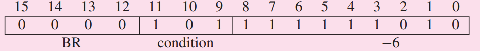
BR(Conditional Branch) may change the contents of the PC.
BR also uses PC+offset as its addressing mode.
- bits[15:12]: opcode 0000<->BR
- bits[11:9]: condition, is used to decide whehter it will change PC or not, the detail will be cover later.
- bits[8:0]: offset, how to calculate the address is the same as that in LD instruction.
Condition Code
Condition code(CC): three single-bit registers.(N for Negative, Z for Zero, P for Positive) Individually set or cleared each time one of the eight GPR is written into as a result of execution of one of the operate instructions or one of the load instructions.
Which instructions will modify the value of CC? See instruction set table where there is a '+' for those instructions or find the answer from the FSM.
During the EXECUTE phase of the BR instruction cycle, the processor examines the condition codes whose associated bits in the instruction, bits[11:9], are 1. If any of the condition codes that are examined are set, the jump!