Import Design and Floorplan
约 3312 个字 20 张图片 预计阅读时间 11 分钟
Abstract
- Moving to the Physical Domain
- A bit about Multiple Voltage Domains
- Floorplanning
- A bit about Hierarchical Design
- Power Planning
Moving to the Physical Domain
- 现在我们基本完成了设计流程的 Front-End,现在要开始 Back-End,从 logical 方法到 physical 方法。
- Floorplan 布局规划,对设计中较大的或重要的部分例如 IPs,I/Os,Power grids,special route,进行空间分配和布局决策。
- Placement,将设计的各个逻辑门和模块(standard cell)放置到芯片上的具体位置。这里会考虑 congestion 和 timing 的问题。
- Clock Tree Synthesis,分配时钟,确保时钟信号能够均匀且同步地到达芯片上的所有触发器。
- Routing 布线,将所有放置好的逻辑门和模块之间的连接线(nets)连接起来,根据 DRC 设计规则检查、timing、noise 等要求进行布线。
- 准备工作:
- Define design (.v)
- Define design constraints/targets (.sdc)
- Define operating conditions/modes (MMMC)
- Define technology and libraries (.lef)
- Define physical properties (Floorplan)
- 在逻辑设计阶段的综合部分,我们认为芯片面对的世界是相对理想的,不考虑电源供应、物理连接和实体、时钟的非理想情况。但是在物理实现,我们要考虑这些物理特性:
- 定义“全局网络”及其如何连接到物理实例。全局网络通常指的是那些需要在整个芯片上传播的信号,如 clk,rst。需要定义这些信号如何连接到芯片上的各个物理实例,例如逻辑单元和宏单元。
- 提供技术规则和单元抽象(LEF 文件
) 。 - 提供物理单元,这些单元对逻辑功能不是必需的,综合的时候往往会禁用这些单元。
- Tie cells: 用于提供逻辑上的高电平或低电平。
- P/G Pads: 用于芯片与外部电源的连接。
- Decaps: 用于电源和地之间的噪声过滤。
- Filler cells: 用于填充芯片上的空白区域,以提高制造良率。
- 定义 hold 约束以及所有操作模式和条件(MMMC
) 。在理想的时钟模型中,保持约束很容易满足,因此通常不会进行检查。但在物理实现中,需要考虑时钟的非理想性,如时钟偏斜和抖动,并定义相应的约束。 - 设置“低功耗”定义,例如电压域、电源门控等。
Multiple Voltage Domains
- Define power domains
- Create power domain names
- List of cells connected to VDD1, VDD2, GND1, 即有哪些 cell 连接该域的电源和地。
- Draw the power domains 电压域。
- Place macros
, (宏单元通常指的是较大的设计模块)考虑 routing congestion、orientation,通常手动指定比自动放置更优。 - Place switches,对于需要电源管理的电源域,需要放置电源开关,用于控制电源域的开启和关闭。
- 为了实现多电压域,我们需要用到 Level Shifter 来转化电压
。 (具体的看不懂) - 为了提高能效比,设计师通常会将芯片划分为多个电源域,每个电源域可以在不需要时关闭电源,从而降低整体功耗。这也就是 Power Gating。
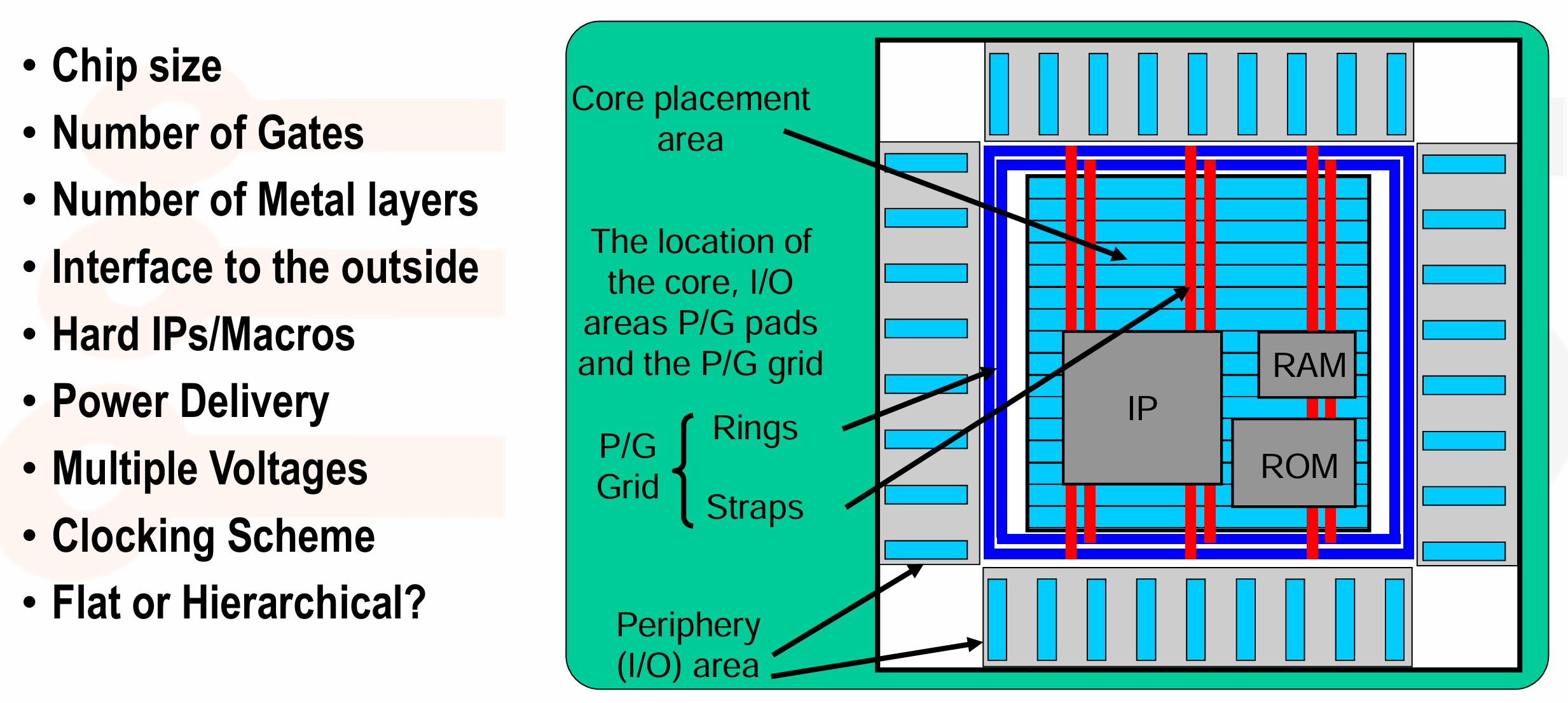
Floorplanning
- Floorplanning is a mapping between the logical description (the netlist) and the physical description (the floorplan).
- Goals of floorplanning:
- Arrange the blocks on a chip.
- Decide the location of the I/O pads.
- Decide the location and number of the power pads.
- Decide the type of power distribution.
- Decide the location and type of clock distribution.
- Objectives of floorplanning are: Minimize the chip area, delay, routing congestion
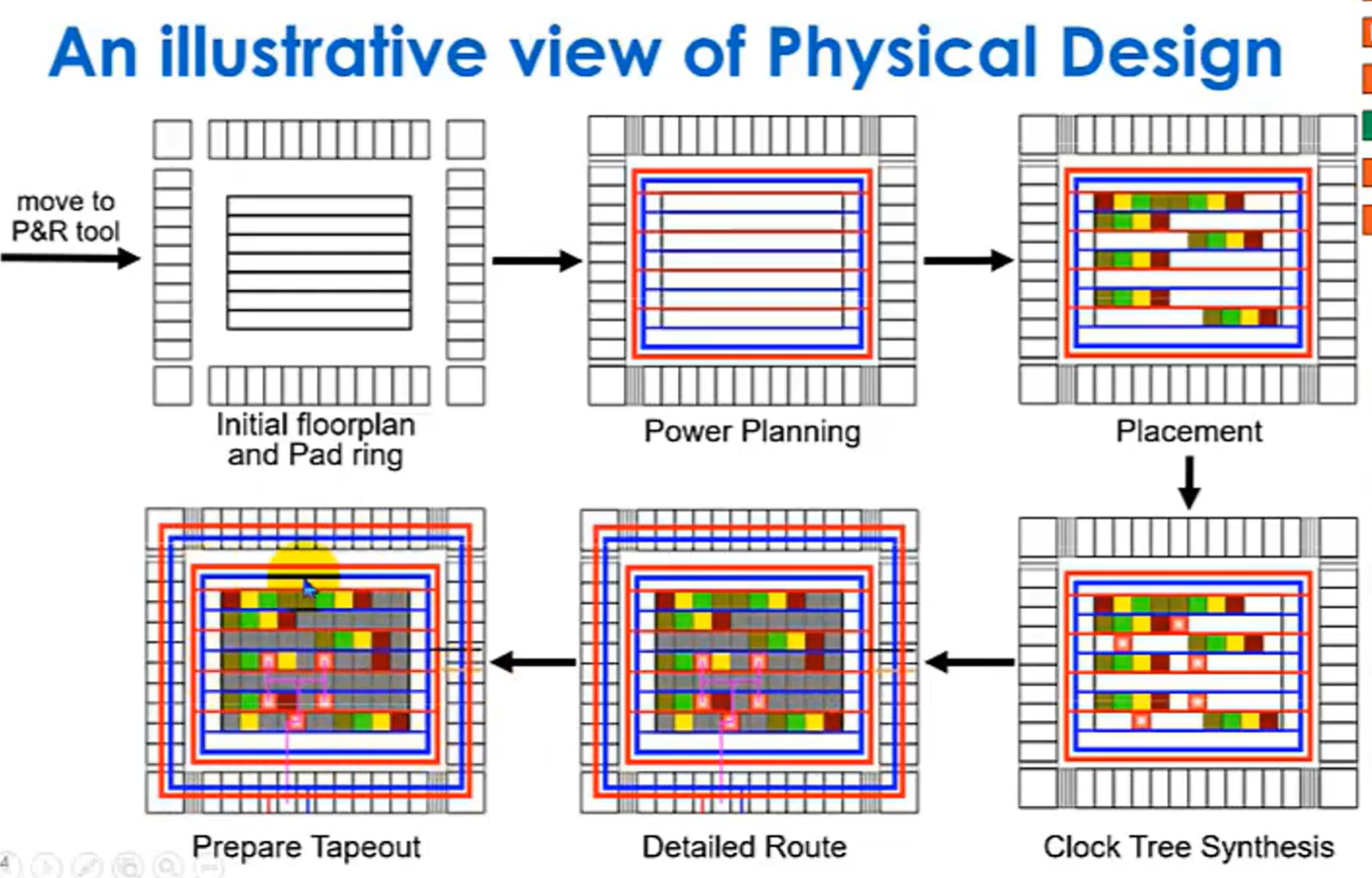
Fullchip Design Overview
-
Floorplanning Inputs and Outputs
- Inputs: Design netlist、Area requirements、Power requirements、Timing constraints、Physical partitioning information、Die size vs. performance vs. schedule trade-off(required); I/O placement、Macro placement information (optional)
- Outputs: Die/block area、I/Os placed、Macros placed、Power grid designed、Power pre-routing、Standard cell placement areas
-
Design ready for standard cell placement
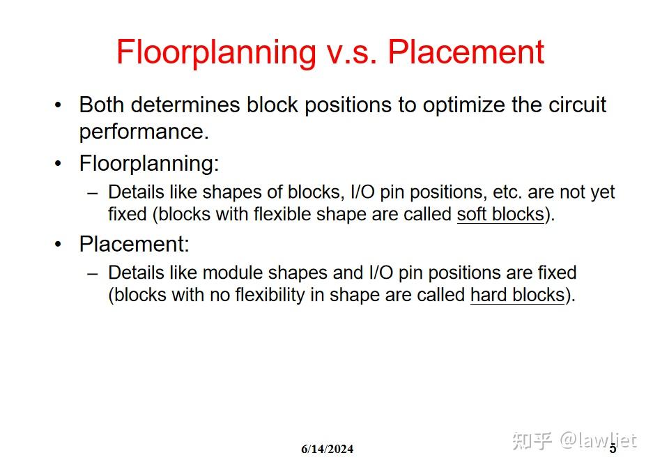
Floorplanning vs. Placement
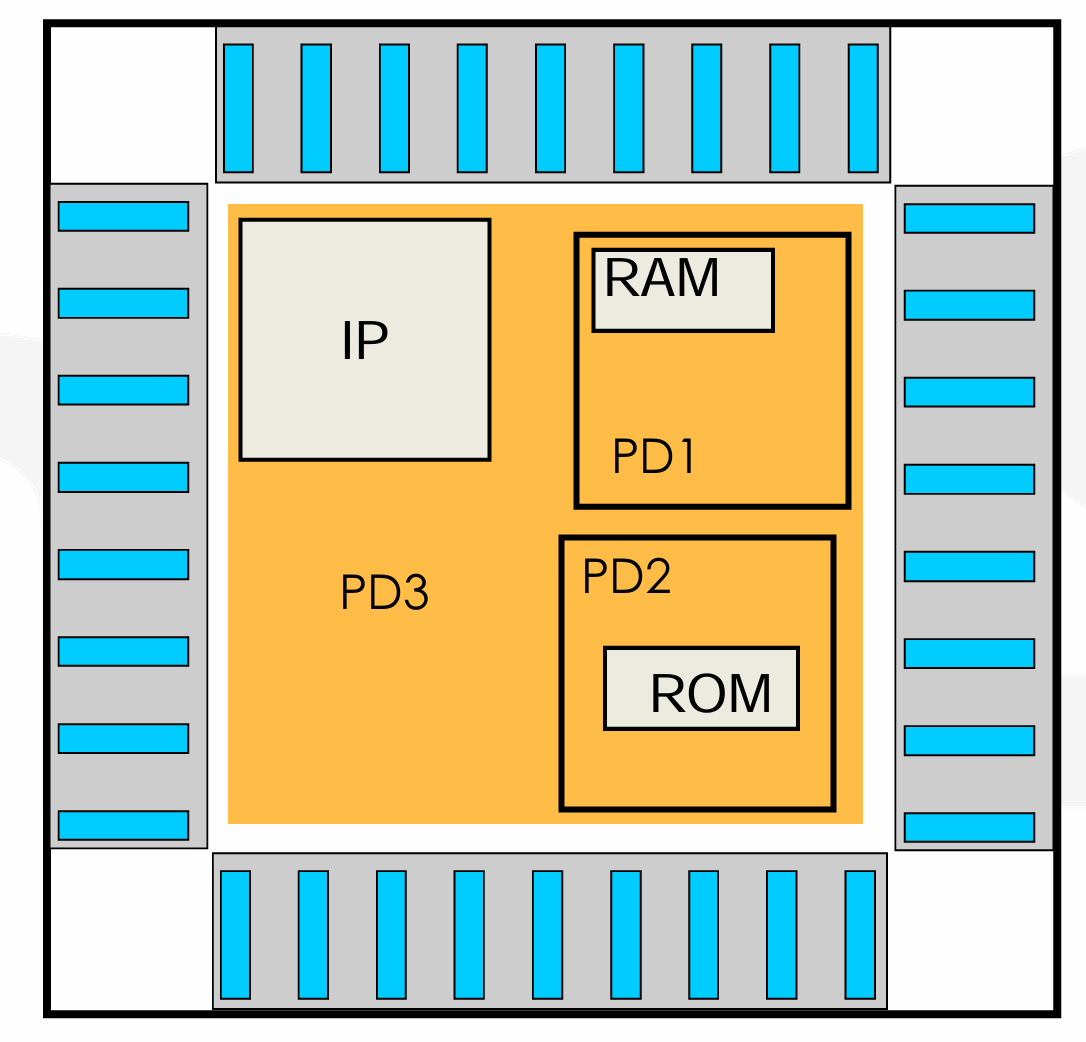
其实 Floorplanning 已经完成了一定的 Placement 工作,通俗来讲,Floorplanning 关注的是芯片的宏观布局,而 Placement 关注的是逻辑单元的微观布局。Floorplanning 为 Placement 提供了一个基本的设计框架,而 Placement 则在这个框架内进行详细的设计优化。
https://pica.zhimg.com/v2-afd4cf6bd21b23d7f016c6a2e754581a_1440w.jpg
-
IO Ring
- I/O RING(I/O 环)是指芯片封装边缘上的一个环形区域,其中包含了芯片与外部世界通信的输入输出引脚。这些引脚可以是数据信号、电源信号、接地信号或其他类型的信号。
- 芯片的引脚分配通常由前端设计师决定。
-
I/O 并没有像 Moore's Law 那样,因此他们的 area 非常大,而且他不仅是链接外部的信号,还会用来提供 power,因此 I/O planning 是 floorplanning 的关键环节。
Chip Size
- Core Limited,在早期,我们的 IO 不大但是 core 很大,因此整个芯片面积取决于 core,核心不够大。
- Pad Limited,现在常见情况,IO 大但是 core 小,因此可以看到中间有很多空白。

-
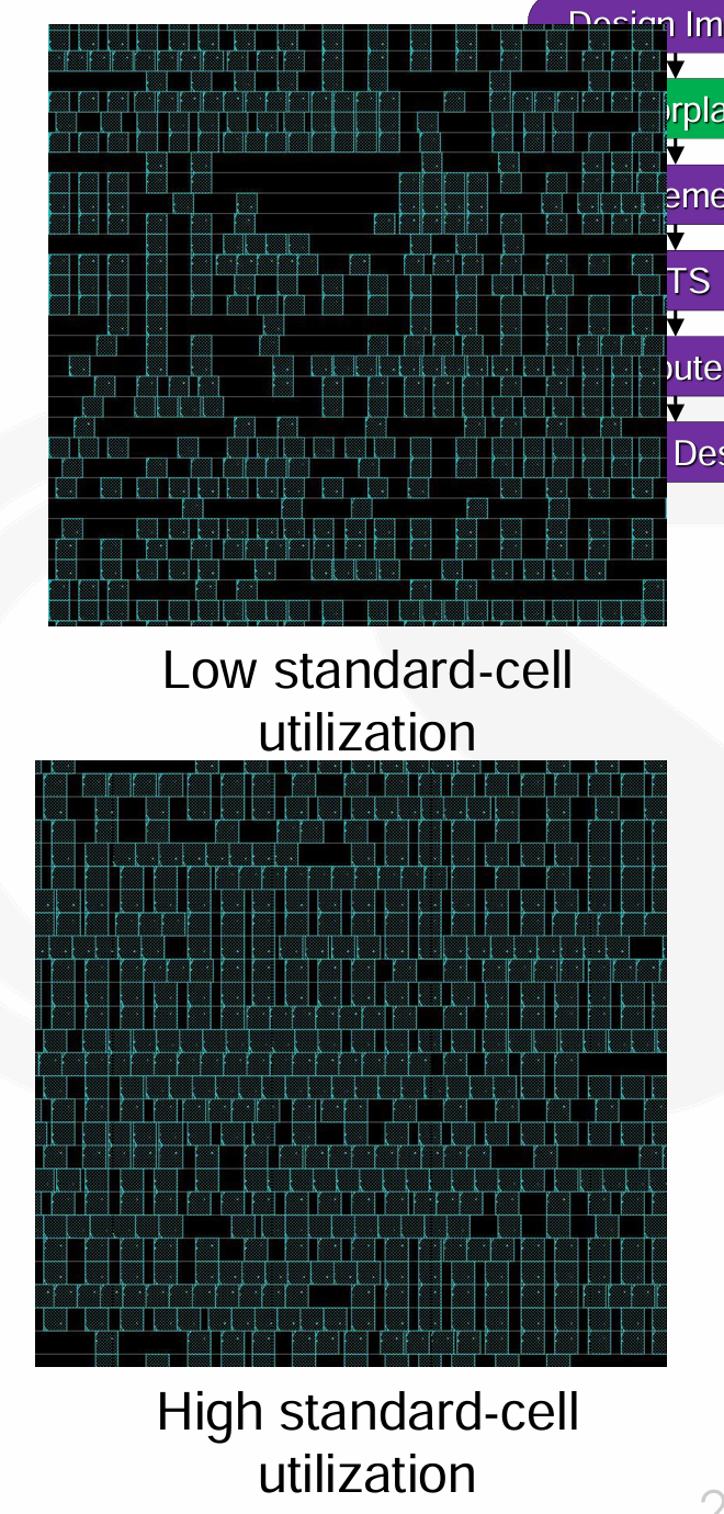
Utilization
- percentage of core area that is taken up by standard cells,通常的起始利用率在 70%,这与设计的关系很大。
-
High utilization can make it difficult to close a design,利用率高可能导致布线拥挤,或者不利于后续优化。
Example
例如下面,当利用率高时,可用的空间小,如果我们希望添加 buffer 或者调整大小,就会很困难。
-
Local congestion 可能发生在一些 pin-dense cells,例如多路选择器。比如一个 4-1 MUX 有 7 个 pin(4 输入 2 选择 1 输出
) 。由于引脚数量较多,可能会在布局时占据较大的空间,从而导致其他逻辑单元的利用率并不完全能反映芯片的实际面积需求。
-
Uniquifying the Netlist
- When moving to the physical domain, the netlist must be unique,在物理设计的时候网表应该是唯一的,即每个子模块只能被引用一次。
- 在 placement 之前,通常由 synthesizer 或者 design import 时完成
, (P&R 前需要检查) ,将对同一个子模块的引用分开。 -
这样做的好处是,P&R 后可能需要对某一个模块进行优化(例如插入 buffer
) ,网表唯一使得这个优化不会影响到其他模块。
-
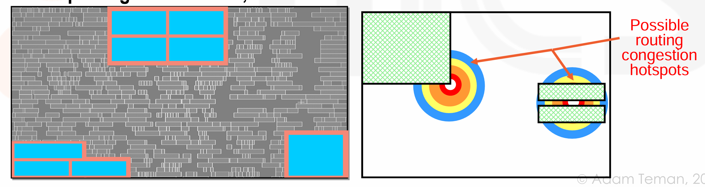
Hard Macro Placement
- 在放很大的 macro 的时候,我们需要考虑他对 routing,timing,power 的影响。通常把他们放在布局的边上。因为 Placement 算法在 single large rectangular 的地方表现得更好。
- 摆放好后,我们把 hard macro 标记为 FIXED,后续不在改动。
Hard Macro Placement
在拐角的地方,如果两侧有 std cell 他们的布线可能也比较困难;如果两个 macro 中间间隙很小,也会有类似问题。这样的地方称为 possible routing congestion hotspots。
-
Placement Regions
- 在芯片设计中为逻辑单元指定特定的放置区域或集群区域,以帮助布局和布线工具更好地实现设计目标。
- 常见的 Place Regions:
- Soft guide, try to cluster these cells together without a defined area.
- Guide, try to place the cells in the defined area.
- Region, must place the cells in the defined area, but other cells may also be placed there.
- Fence, must place the cells in the defined area and keep out all other cells.
-
在实践中,使用 regions 不一定能带来好的结果。
Example
-
Placement Blockages and Halos
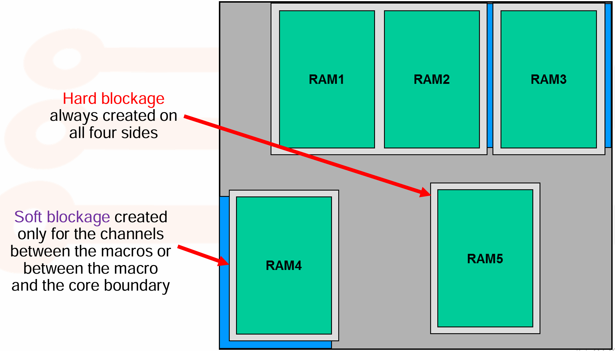
- Placement Blockages 是芯片设计中需要特别注意的区域,这些区域不允许逻辑单元放置。
- 常见的 Blockages 包括:
- Hard Blockage, no cells can be placed inside.
- Soft Blockage, cannot be used during placement, but may be used during optimization.
- Partial Blockage, an area with lower utilization.
-
Halo (padding),an area outside a macro that should be kept clear of standard cells,设置 Halos 的目的是为了保护芯片的边缘区域,防止逻辑单元过于靠近边缘,从而影响芯片的封装和性能。
Example
-
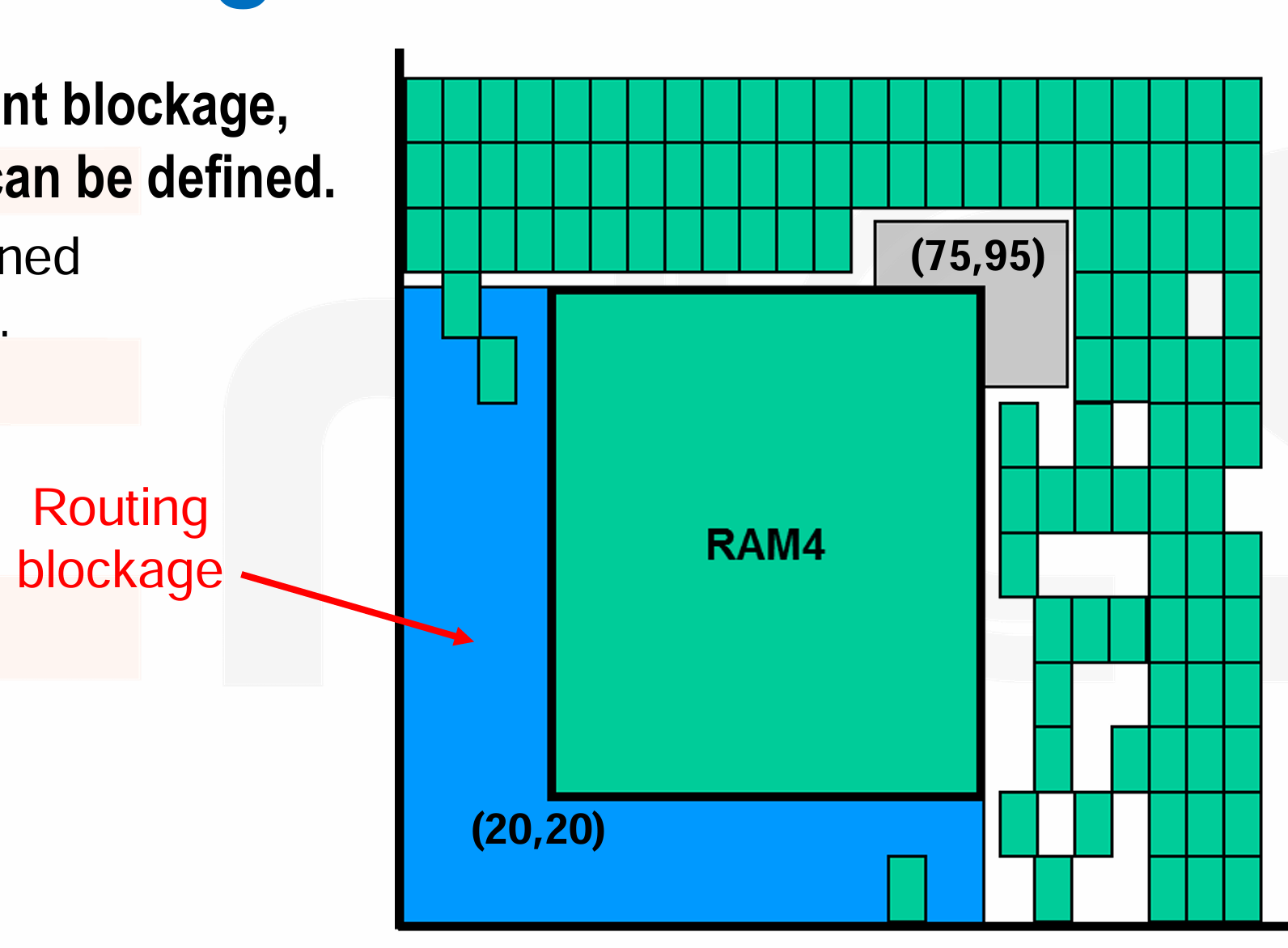
Routing Blockage
-
Similar to placement blockage, routing blockage can be defined,不常用。
Example
-
Guidelines for a good floorplan
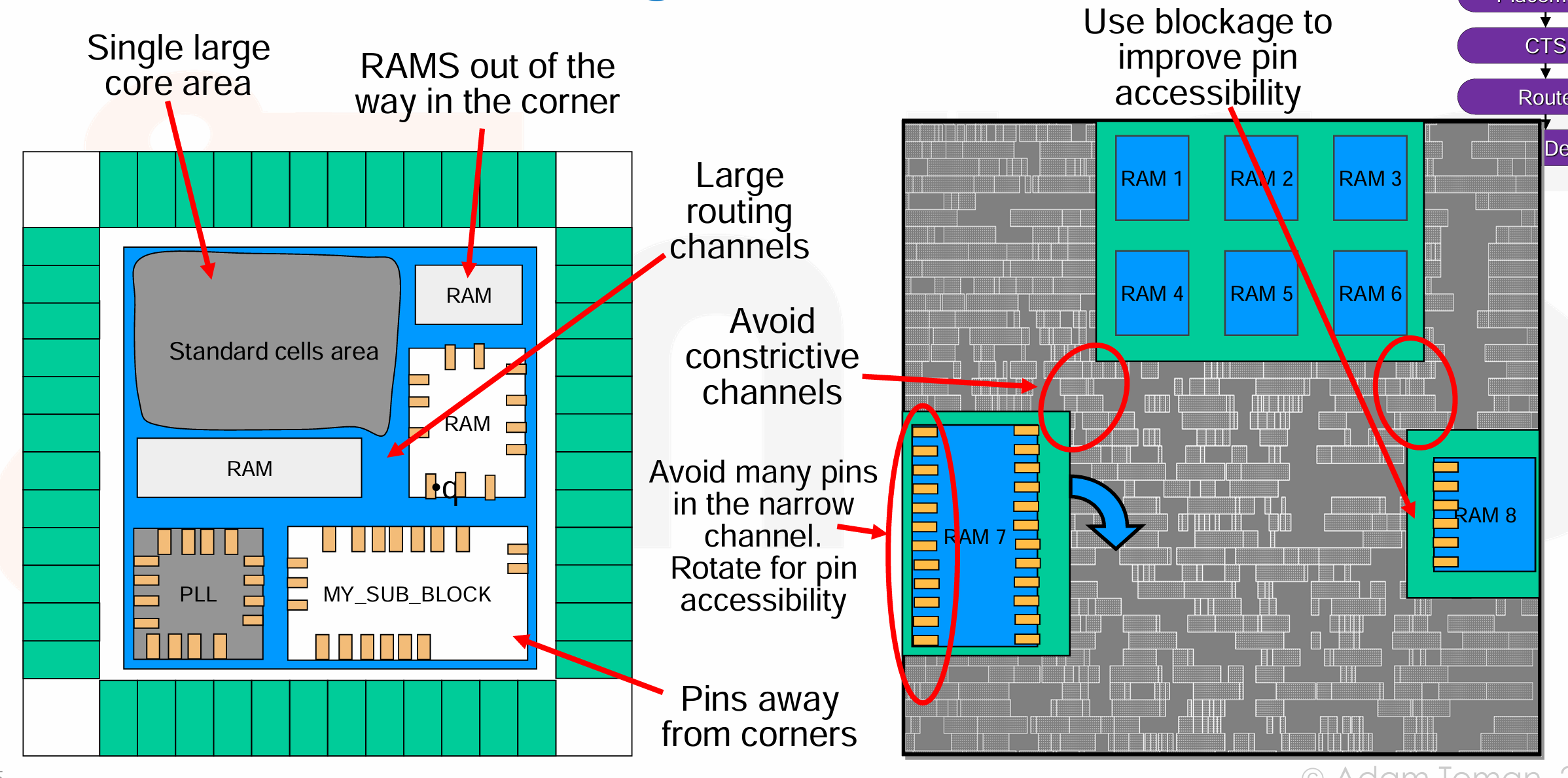
- Single large core area:将逻辑核心区域(如处理器核心、内存模块等)设计为一个单一的大型区域,这样可以减少互连的复杂性,提高性能;
- RAMS out of the way in the corner:将存储器单元放置在芯片的角落或边缘,这样可以减少它们对核心逻辑区域的干扰,同时保持核心区域的连通性;
- Large routing channels:在芯片布局中保留宽大的布线通道,这样可以减少布线拥塞,提高信号的传输效率;
- Avoid constrictive channels:避免在布局中创建狭窄的布线通道,这样可以减少信号的延迟和干扰,提高信号质量;
- Avoid many pins in the narrow channel:在布局中避免在狭窄的通道中放置太多的引脚,这样可以减少布线冲突,提高信号的传输效率;
- Rotate for pin accessibility:根据引脚的访问需求,考虑旋转芯片的布局,以便于引脚的布局和布线;
- Pins away from corners:将引脚远离在芯片的边缘或角落,这样可以减少引脚与芯片边缘的干扰,提高引脚的布局和布线效率;
- Use blockage to improve pin accessibility:在布局中使用 blockage 来改善引脚的访问性,例如,将引脚放置在障碍物附近,以便于引脚的布局和布线;
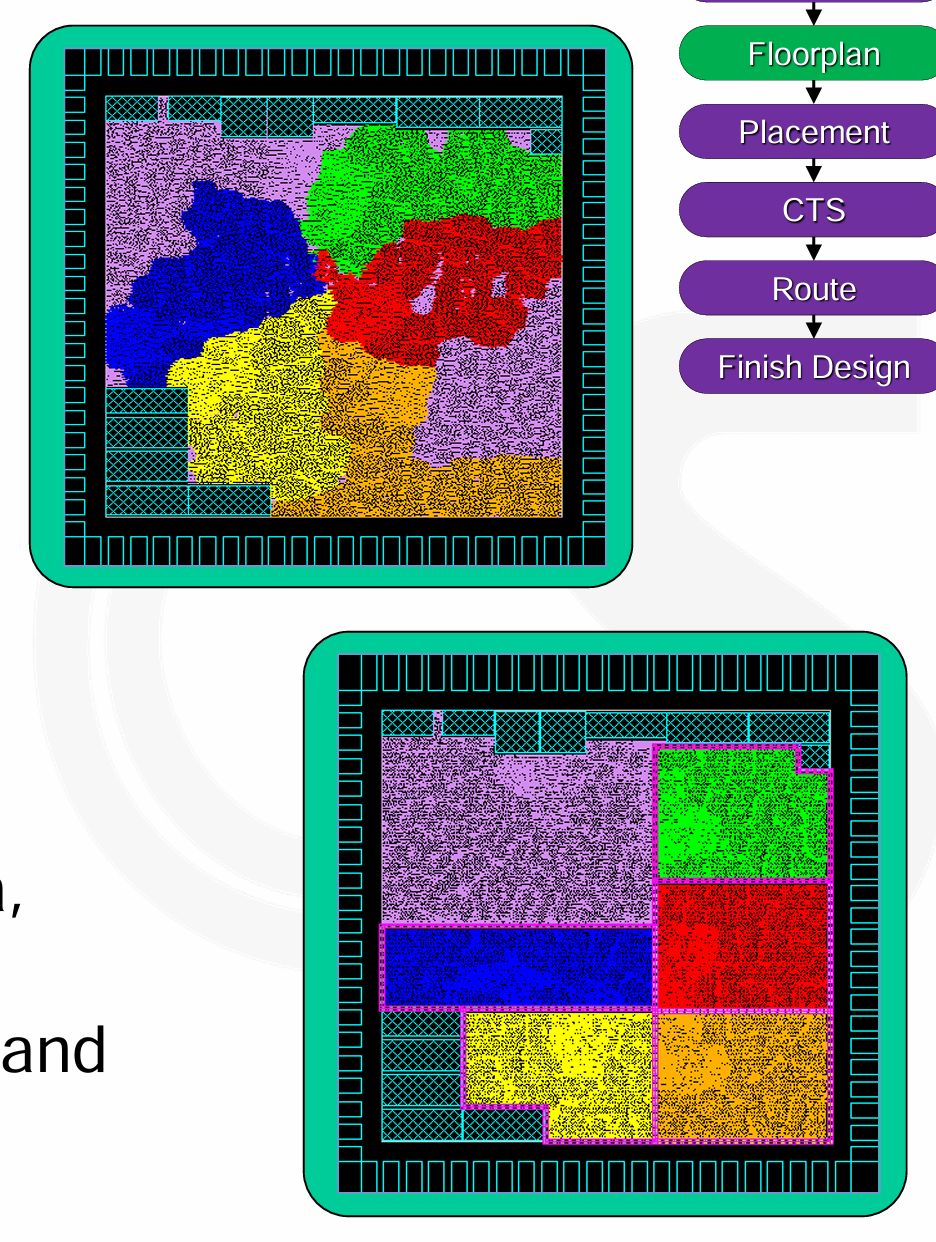
Hierarchical Design
-
如果设计太大的话,我们可以把他分为多个 hierarchies。
- 好处是更快的运行时间,更少的内存消耗(EDA 工具
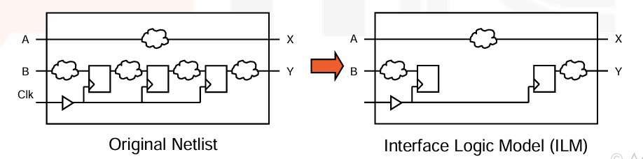
) ,更快的 ECO turnaround time,能够做复用(即相同的 hierarchy 可以在不同的设计中使用) 。 - 缺点是更能实现 fullchip timing closure(ILMs
) ,因为需要确保所有子模块的时序都能满足要求;需要生成 feedthrough、repeater insertiom、timing constraint budgeting 等,以确保时序收敛。
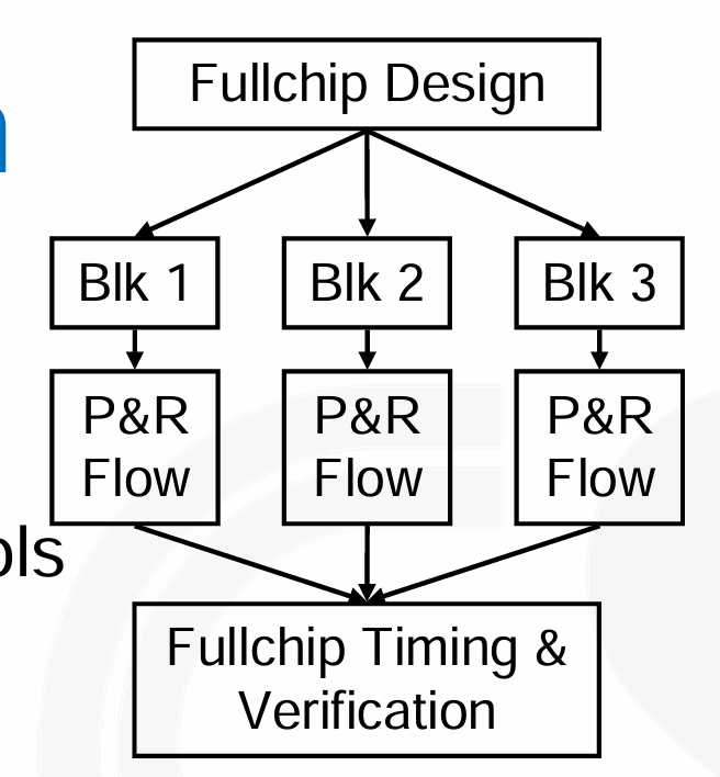
- 好处是更快的运行时间,更少的内存消耗(EDA 工具
Time Budgeting
- 在层次化设计中,chip-level 的时序约束需要正确地映射到各个 block-level 约束。例如某个关键路径的时延不超过某个值,那么这个约束需要被分解并分配给相关的块级时序约束。
-
Interface Logic Models (ILMs) 接口逻辑模型可以简化并加速设计。因为我们 block-level 内部的时序已经在子模块里检测,在分析时可以将中间逻辑简化,相当于只分析 in2reg、reg2out、in2out 的时序。
Pin Assignment
- Pin constraints: Layers, spacing, size, overlap; Net groups, pin guides
- Net groups,将具有相似特性或连接需求的引脚分组。
- Pin guides,用来影响特定 net groups 的自动化 pin 放置。
- Pin 可使用以下两种优先级的约束:
- Placement based:使用 flightlines 来指导引脚的放置,确保它们在芯片上的布局符合特定的规则。
- Route based:指定 trial route 尝试布线和 boundary crossings,以指导引脚的布线路径。
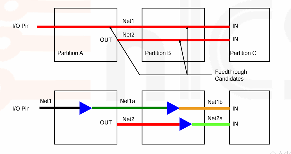
Feedthrough
-
Feedthrough 路径定义从顶层 I/O 引脚进入和穿过 Block,以减少长路由和拥塞。buffer 需要被添加到这些路径中,以保持信号强度并避免 max slew 和扇出违规。
Power Planning
- Power Planning 一般在 floorplanning 阶段完成,placement 阶段可能会有调整。
-
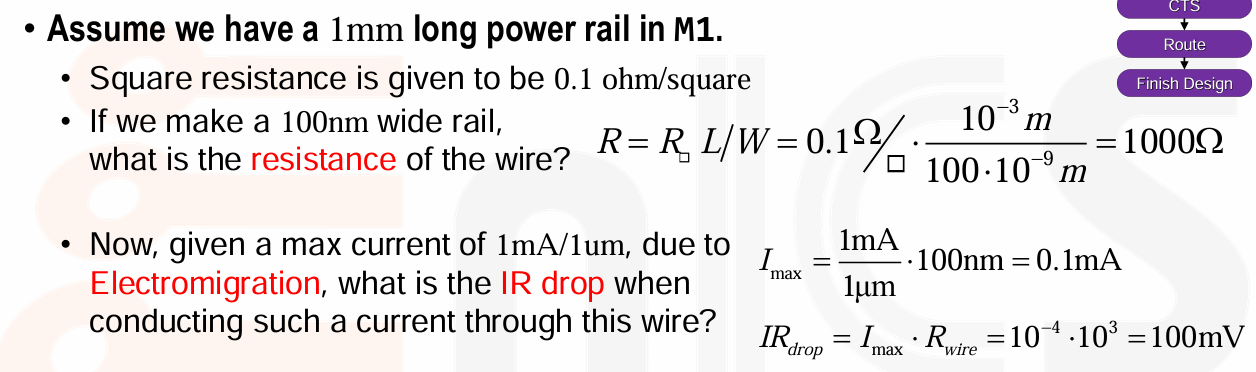
power 由 dynamic 和 static(leakgae) 组成,我们需要考虑电源的 reliability,主要有下面两个问题:
- IR Drop,在电源线(power line)长度上,由于电源线电阻导致的电源电压(supply voltage)下降。
- 构建 resistance matrix,其中包含 power grid 电源网络中每个节点的电阻。
- 考虑每个门的 average current。
- 使用矩阵求解的方法来计算每个节点上的电流。通过矩阵求解,设计者可以确定电源线上的电压下降。
- Electromigration(EM
) ,在集成电路后段会部署大量金属连线结构,本来这些金属连线的作用就是让电子迁移,实现导电。但反过来,电子的流动会造成金属材料迁移,最终导线被“掐断”。- 可能导致短路、开路。或者导致性能的下降(改变 wire RC
) 。
- 可能导致短路、开路。或者导致性能的下降(改变 wire RC
- IR Drop,在电源线(power line)长度上,由于电源线电阻导致的电源电压(supply voltage)下降。
-
Power Distribution Network
- 功能:
- Carry current from pads(焊盘)to transistors on chip,电流从芯片的 IO 端口传输到内部的逻辑单元。
- Maintain stable voltage with low noise
- Provide average and peak power demands
- Provide current return paths for signals
- Avoid electromigration & self-heating wearout
- Consume little chip area and wire
- Easy to lay out
- 更宽的 Power Lines,可以降低 IR DROP,可以减少 EM。但同时会导致 routing 变得困难。
Example
设计者通常会尽可能地使电源轨宽和厚,可以降低电流密度,以减少 EM 和 IR Drop 的影响。
Example
我们使用 color map 来映射芯片的 IR drop,强调 hotspots。可以看到在添加 single wire 之后,IR drop 有所减少。

- 功能:
-
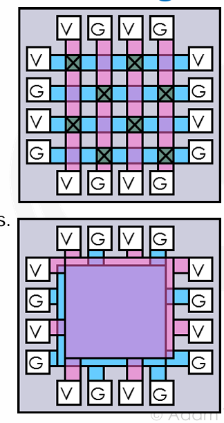
Power and Ground Routing
- 每个 std cell 都要有 power(VDD)和 ground(GND)的连接。
- Power/Ground mesh 允许电源和地信号通过多个路径从源到达目的地。这样有更小的串联电阻,从高层金属层到低层金属层形成一个层次化的 mesh 网络,在不同层之间需要多个通孔(vias)来连接电源和地网络。
- 通常 P/G routings 是很规则的(均匀分布,以提供稳定供应
) ,resources 通常会预留出来。
-
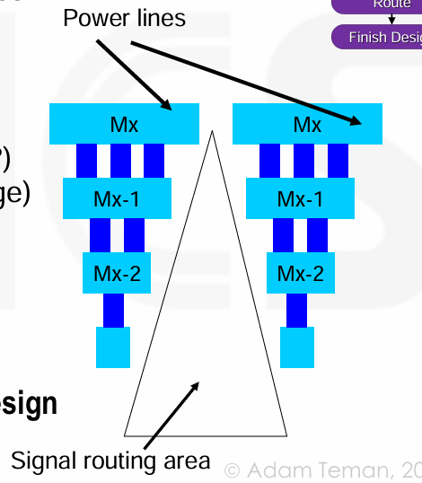
Standard Approaches to Power Routing
- Power Grid,通过水平和竖直的 power bars 互联;在大部分高性能设计中使用;Often well over half of total metal on upper thicker layers used for VDD/GND
-
Dedicated VDD/GND planes,成本昂贵,只在 Alpha 21264 使用过。
-
Power Grid Creation
- 权衡 IR drop, EM VS. routing resources
-
Need to determine: General grid structure (gating or multi-voltage?), Number and location of power pads (per voltage), Metal layers to be used, Width and spacing of straps, Via stacks versus available routing tracks, Rings / no rings, Hierarchical block shielding.
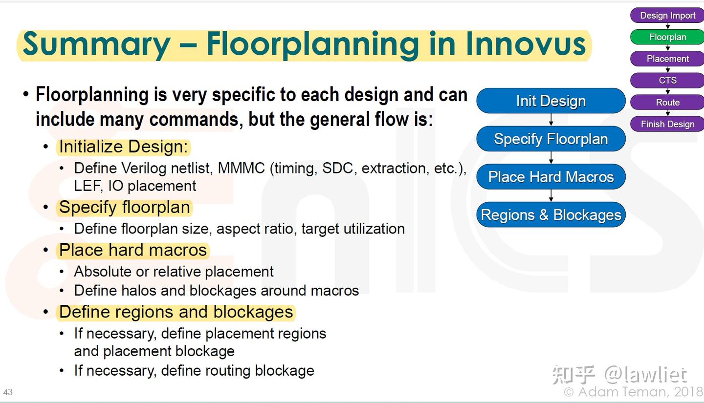
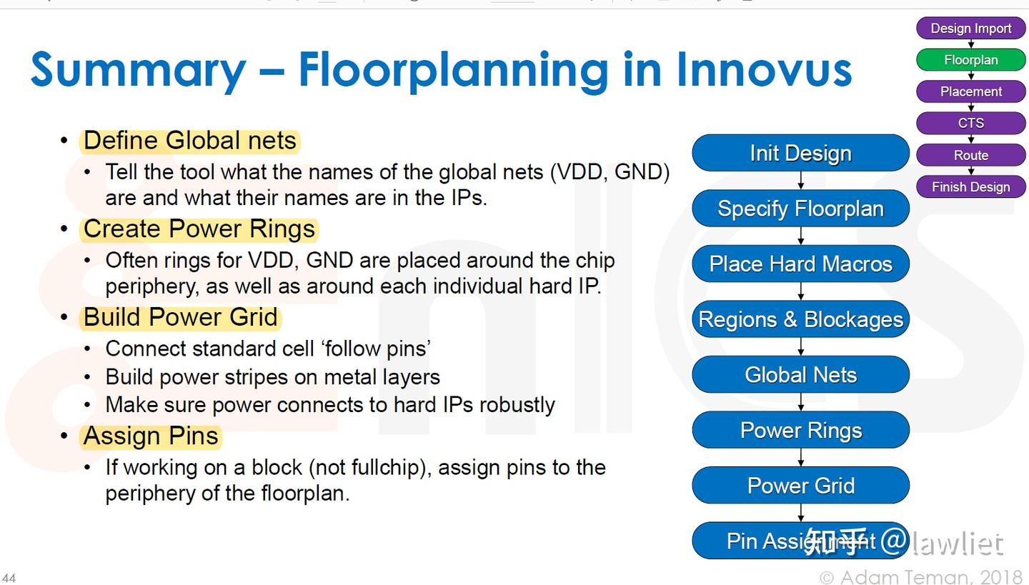
Floorplanning in Innovus