Chapter 3 Digital Logic Structures
约 1706 个字 26 张图片 预计阅读时间 6 分钟
Abstract
Covered in Lecture 2, 2022.7.12 and Lecture 3, 2022.7.13
Topics:
1. Transistors
2.
Transistors
- N-type
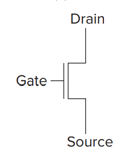
Gate 通 1.2V 的时候导线接通 (short circuit), 通 0V 时导线断开 (open circuit).
其中 Gate 称作栅极, Drain 称作漏极, Source 称作源极.
- P-type
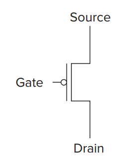
Gate 通 0V 的时候导线接通 , 通 1.2V 时导线断开 .
Note
P-type: P 断 N 通
N-type: N断P通
其中 P 指 Positive(1.2V/接电源正极)
其中 N 指 Negtive(0V/接地/接电源负极)
Logical Gates
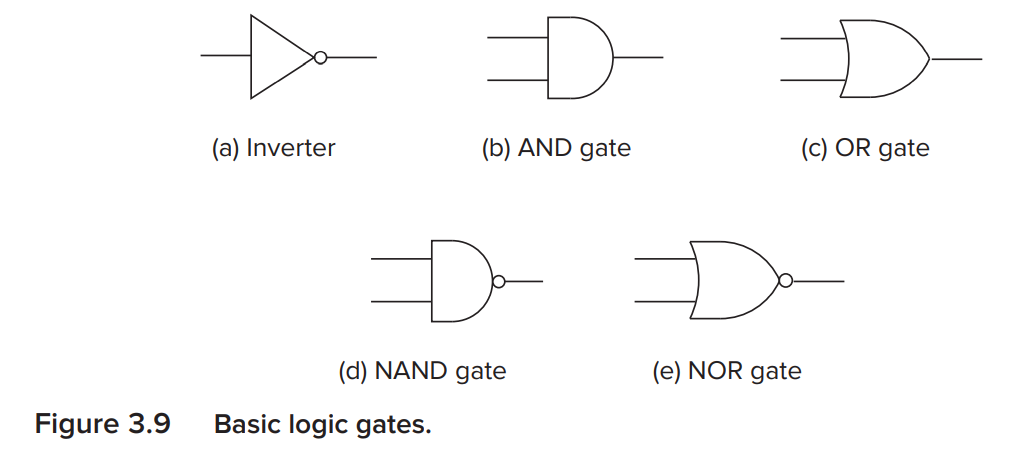
其中可以直接用小空心圆表示 " 非 ".
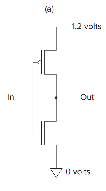
The Not Gate(Inverter)
| In | Out |
|---|---|
| 0 | 1 |
| 1 | 0 |
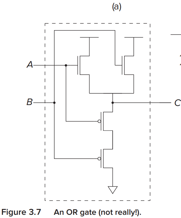
OR and NOR Gates
NOR Gate
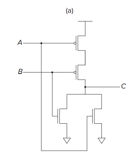
为什么不可以直接将 P-type 直接接地 ?
这样 C 始终和地接触 , 当 A, B 的值均为 0 时 , 上方也会接通 . 这样 C 会同时和高低电压接通 . may burn the house!(by Patt)
OR Gate
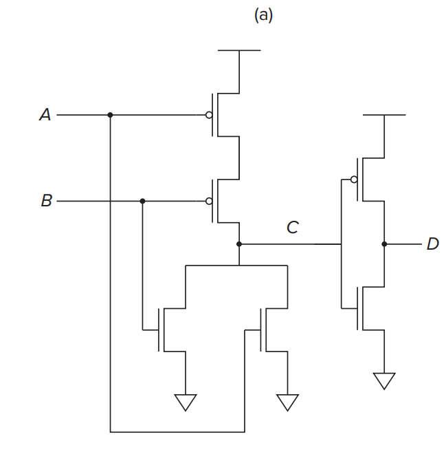
| A(in) | B(in) | C(NOR) | D(OR) |
|---|---|---|---|
| 0 | 0 | 1 | 0 |
| 0 | 1 | 0 | 1 |
| 1 | 0 | 0 | 1 |
| 1 | 1 | 0 | 1 |
Question
但 P 型 mos 晶体管的源极必须接正极 , 漏极必须接负极 . 否则会有传输电压损失 .
AND and NAND Gates
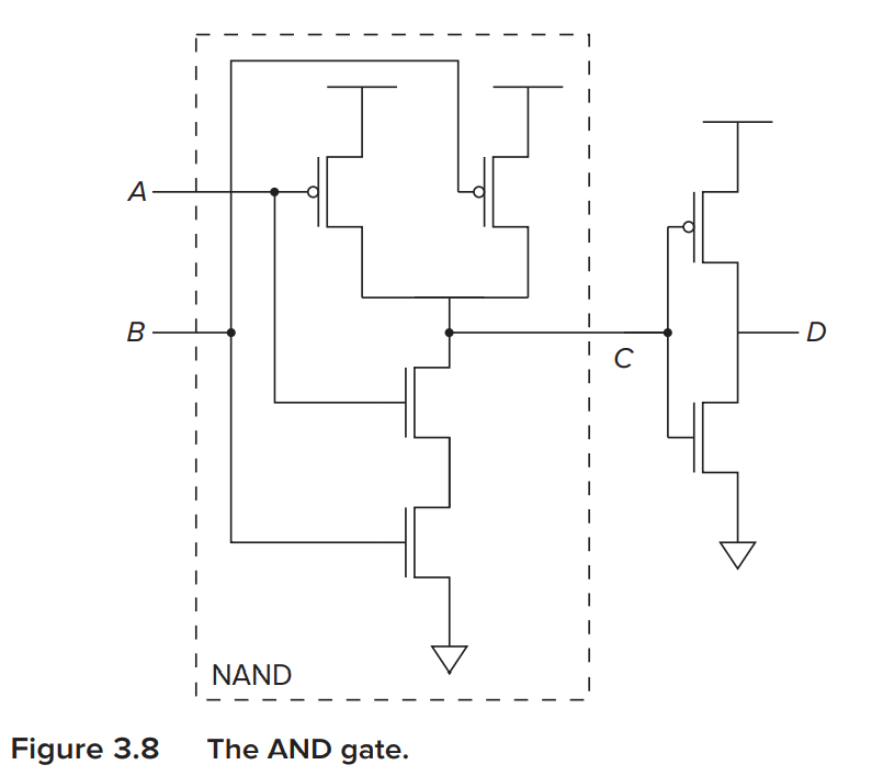
| A | B | C(NAND) | D(AND) |
|---|---|---|---|
| 0 | 0 | 1 | 0 |
| 0 | 1 | 1 | 0 |
| 1 | 0 | 1 | 0 |
| 1 | 1 | 0 | 1 |
Combinational Logic Circuits
property: only about Right now, means their result is independent on the any past information stored in memory.
Decoder( 译码器 ) 
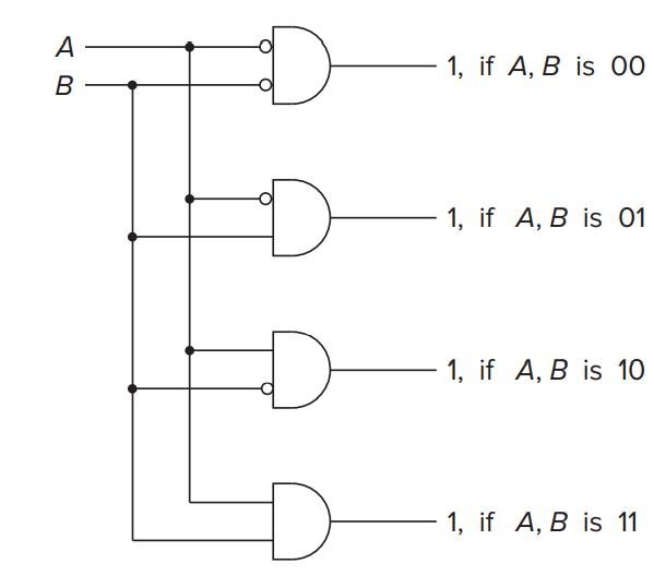
n input, \(2^n\) outputs, only one output is logically 1 correspounding to the input pattern.
Mux(Multiplexer 数据选择器 ) 
The funtion of a mux is to select only one of the input and connect it to the output.
Example
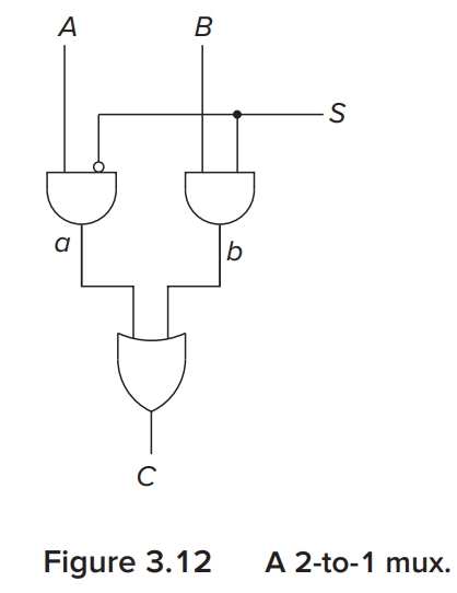
\(S=0\), C 输出 A 的值 ; \(S=1\), C 输出 B 的值 .
简写为:
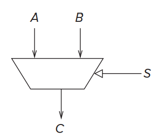
In general, a mux consist of \(2^n\) inputs and n select lines.
\(2^n\) 个输入对应各不相同的选择线的组合(n 条线有 \(2^n\) 种组合), 对于给定的一个 S(n bits), 有且仅有一个输入被选中.
Info
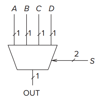
线上的一撇加数字表示信号的位数 . e.g. 图中 ABCD 都是一位的输入信号 , 但选择信号 S 为两位 .
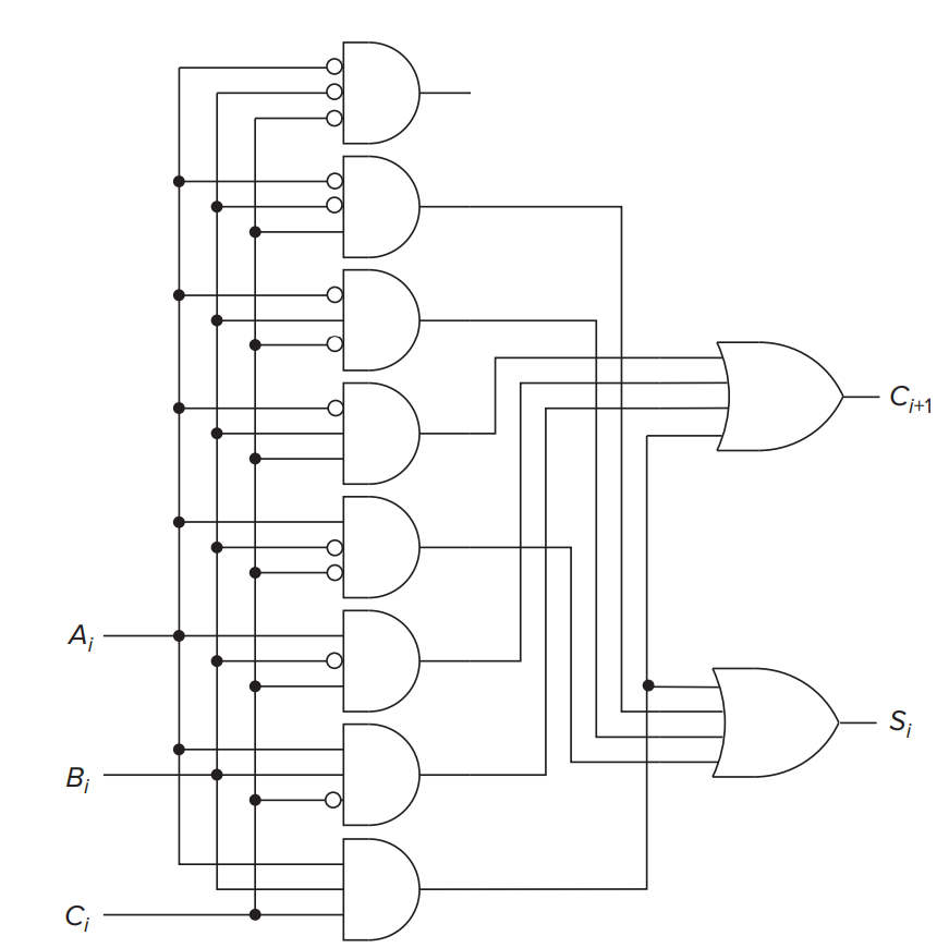
One-Bit Adder(Full Adder)
| \(A_i\) | \(B_i\) | \(C_i\) | \(C_{i+1}\) | \(S_i\) |
|---|---|---|---|---|
| 0 | 0 | 0 | 0 | 0 |
| 0 | 0 | 1 | 0 | 1 |
| 0 | 1 | 0 | 0 | 1 |
| 0 | 1 | 1 | 1 | 0 |
| 1 | 0 | 0 | 0 | 1 |
| 1 | 0 | 1 | 1 | 0 |
| 1 | 1 | 0 | 1 | 0 |
| 1 | 1 | 1 | 1 | 1 |
其中 \(A_i, B_i\) 表示 A/B 的第 i 位 , \(S_i\) 表示执行加法之后第 i 位的值 , \(C_{i+1}\) 表示是否有进位 .
A circuit for adding two 4-bit binary numbers using block above.
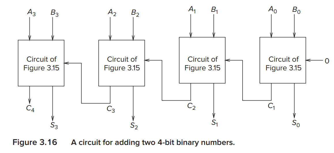
其中 , 最右边的一个电路相当于是半加器 (half adder), 因为他相当于没有进位 (carry=0), 另外三个电路是全加器 .
PLA(the Programmable Logic Array)
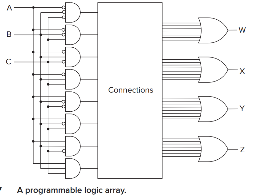
其中 \(2^n\) 个输入 , 经过 Decoder 得到输入的组合 . 最后得到我们希望生成的函数 .
Logic Completeness
{AND, OR, NOT} is logically complete because we can buile a circuit to carry out the specification of any truth table without other kind of gate(by PLA).
!!! Question Is NAND logically completeness?
Yes.
\(P\ NAND\ Q=NOT (P\ AND\ Q)\)
so \(P\ NAND\ P=NOT\ P\), \(P\ AND\ Q=NOT(P\ NAND\ Q)\), \(P\ OR\ Q=(NOT\ P)\ NAND (NOT\ Q)\)
Basic Storage Elements
The R-S Latch(RS 锁存器 ) 
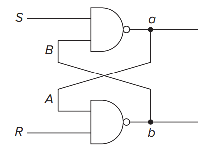
其中 a 既是我们存储的值 , 也是我们要输出的值 (a 输出 Q, b 输出非 Q).
工作过程:
- 起初 \(S=R=1\), 处于混沌状态 , 不知 a/b 的值 .
- 使用时 :
- 把 S(set) 拨一下到 0, 则 a->1, 成功将 1 存入 .
再把 S->1, 此时 \(S=R=1\) 处于正常工作状态, 只要 S/R 不改变, 存储的值就不会改变. - 把 R(reset) 把 0, 则 a->0, 成功将 0 存入 .
再把 R->1, 回到正常工作状态. - 非正常工作状态 : \(S=R=0\), 混沌状态 , 而且此时 \(a=b=1\), 不满足 Q 与非 Q 的定义 , 此时电路的输出取决电路的性质 .
| R | S | Q | 非 Q | |
|---|---|---|---|---|
| 1 | 1 | ? | ? | Unknown |
| 0 | 1 | 1 | 0 | Set |
| 1 | 1 | 1 | 0 | The latch "remenber" the value |
| 1 | 0 | 0 | 1 | Reset |
| 1 | 1 | 0 | 1 | The latch "remenber" the value |
| 0 | 0 | 1 | 1 | Both go to high |
| 1 | 1 | ? | ? | Unknown |
The Gated D Latch(D 锁存器 ) 
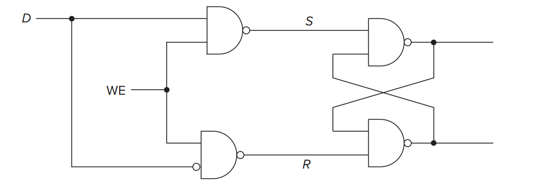
WE: Write Enable.
- WE is asserted(WE=1, can write): D->1, S=1 R=0, 1 is stored. D->0, S=0 R=1, 0 is stored. Thus, we can think that the Gated D Latch store the value of D.
- WE is not asserted(WE=0, only read): R=1 S=1, so whether D is 0 or 1 it cannot change the stored value.
The Concept of Memory
Address Space
We refer to the unique identifier associated with each memory location as its address.
We refer to the total number of uniquely identifiable locations as the memory’s address space.
Addressability
We refer to the number of bits of information stored in each location as its addressability.
For \(2^n\)-by-m-bit memory, its address space is \(2^n\) while its addressability is m.
Example
假设玉湖七幢 6 楼为一块内存 , 其中这一楼一共有 20 间寝室 , 这就是内存空间 .( 因为每间寝室都有独一无二的寝室号 )
而每间寝室都是四人间, 因此可寻址能力是 4, 表示最小的寻址单元.
A \(2^2\)-by-3-Bit Memory
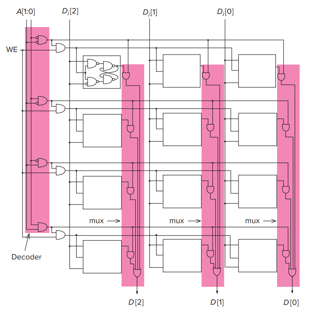
其中 A[] 表示地址 , D[] 表示数据 .(A[1:0] 可以理解为 Python 里的 list)
- 从 A[1:0] 中输入地址 , 通过 Decoder 对应某一行 . 其中每一行为 3 bits, 因此有三个存储器 .
- WE=0 时读取数据 , 此时每个 bit 中的存储器 (R=S=1, 只能读 ) 将其中的值读出 , 通过 mux 最后输出出来得到 D[2:0].
- WE=1 时写入数据 , 此时每个 bit 中为 D 锁存器 , 由上文可知会直接写入 D 的值 , 即 \(D_i[2:0]\). 此时也会有输出 .
Sequential Logic Circuits
property: they contain store elements to keep track of prior history information.
State
The state of a system is a snapshot of all the relevant elements of the system at the moment the snapshot is taken.
Finite State Machine
A finite state machine contains:
- A finite number of states.
- A finite number of external inputs.
- A finite number of external outpus.
- An explicit specification of all state transitions.
- An explicit specification of what determines each external output value.
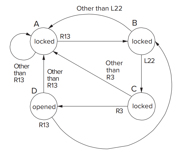
Combination lock
我们需要依次拨到 R3-L22-R13(L/R 代表拨的方向 ), 锁才能打开 . 否则如 R13-L2-R 也是不能打开锁的 .
state machine:
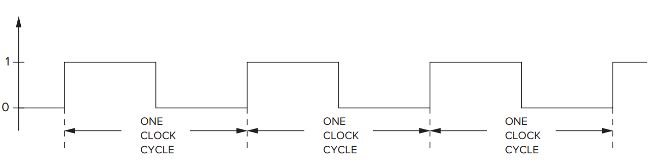
The Synchronous Finite State Machine
In the example above, there is no fixed amount of time between successive inputs to the finite state machine, which means we can dial R3 and wait for a day then dail L22. (asynchoronous) However, computers work in synchronous way because the state transistions take place, one after the other, at identical fixed units of time.
Example:A Danger Sign

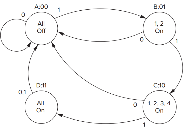
起初 , 1-5 号灯处于关闭 . 当开关处于 ON 状态时 , 第一个单位时间后 1, 2 灯亮 ; 第二个单位时间后 3, 4 灯亮 ; 第三个单位时间后 , 5 灯亮 .
状态机:
其对应的电路 :
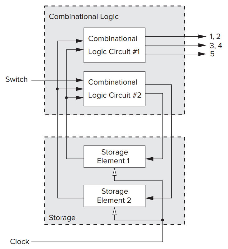
其中 store element 1 存储低位 , element 2 存储高位 .
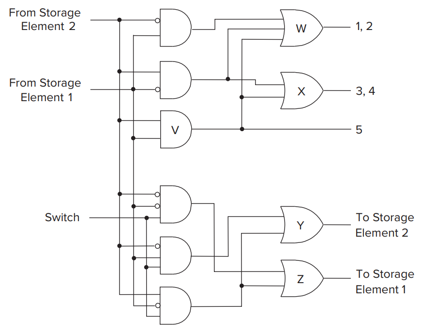
由此得到的组合电路 :( 可通过真值表得到 )
But in the previous example, there is a question: The process is so fast that the input of next cyle will be the output of the last cycle almost immediately. So we have no idea what the state of the finite state machine woule be for the next clock cycle.
Master-Slave Flip-flop
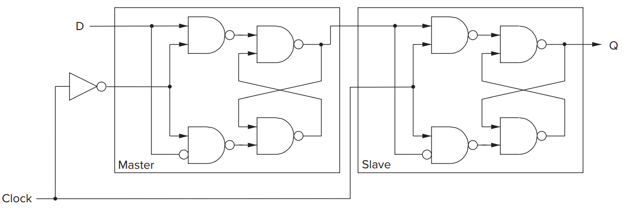
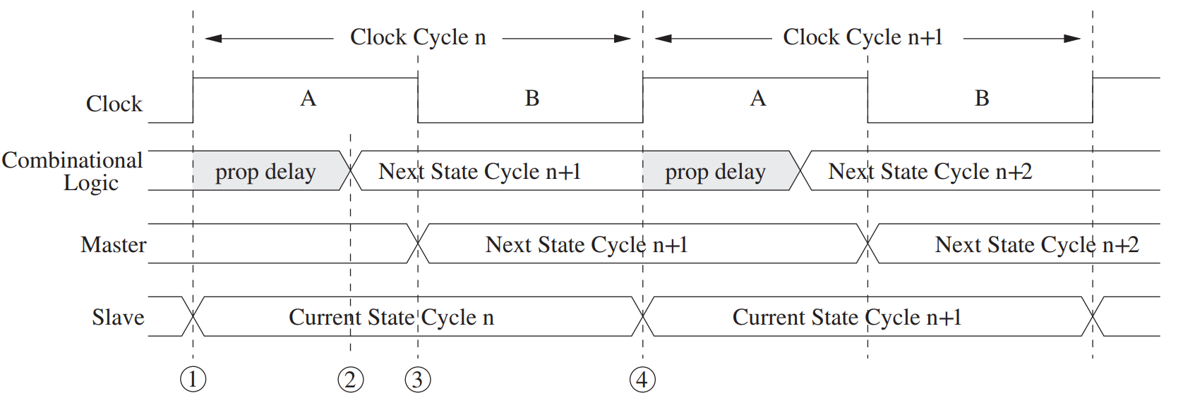
process:
- In the first half A(WE=1), the slave read the value from the master and update the value by combinational circuits(Q) while the master remain the same.
- In the second half B(WE=0), the value updated by combinational circuit is stored in master while the slave remain the same.
-
Timing diagram
-
the slave load the value from the master.
-
the combinational logic finishes its update/calculation(proper delay). So it enters the next cycle.
-
the master load the updated value, so it also enters the next value.
-
repeat 1
-