Sequential Circuits
约 4204 个字 50 张图片 预计阅读时间 14 分钟
Abstract
- 时序电路概念和组成
Introduction to Sequential Circuits - 输出方程、激励函数、次态方程、输出方程类型
Output function, Excitationfunction, Next state function, type of output functions - 时序电路类型
Types of sequential circuits - 电路延迟模型
Circuit delay model -
锁存器与触发器
Latch and Flip-Flop- S-R 锁存器的原理、特征表、特征方程,内部电路分析,不确定状态的原因及出现条件
Analysis of Basic S-R Latch, Characteristic Table, Characteristic Equation, reason of unstable state - D 锁存器、D 触发器的原理、特征表、特征方程,内部电路分析
Theory of D Latch and D Flip-Flop, Characteristic Table, Characteristic Equation - JK 触发器、T 触发器的行为、特征表、特征方程
Behavior of JK Flip-Flop, TFlip-Flop, Characteristic Table, Characteristic Equation - 脉冲触发和边沿触发的概念,脉冲触发的一次性采样行为原因
Concept of Master-slave and edge-triggered flip-flop, 1s catching of Mast-slave flip-flop - 锁存器和触发器的时序,建立时间、保持时间、传输延迟等各种时序成分
Flip-Flop Timing Parameters, setup time, hold time, propagation delay - 各种触发器的图形符号
Symbols of Flip-Flops
- S-R 锁存器的原理、特征表、特征方程,内部电路分析,不确定状态的原因及出现条件
-
状态表、状态图
State Table, State Diagram -
同步时序电路分析
Sequential Circuit Analysis- 根据给定电路,写出输出方程和激励函数 / 次态方程
Derive output functions and excitationfunction/Next state function - 列出状态真值表
ObtainState truth table - 列出时序电路的次态
List next state of sequential circuit - 作状态表和状态图
ObtainState Table and State Diagram - 分析时序电路的外部性能
Analysis the behavior of sequential circuit - 对电路进行评述,通常需检查自恢复功能及画出时序波形图
Evaluate the circuit, validate the self-recovery ability
- 根据给定电路,写出输出方程和激励函数 / 次态方程
-
电路和系统级时序分析,时序电路各路径的时序成分分析计算
Circuit and System Level Timing, analyze and compute time component along any path of the sequential circuit
9.米利型和穆尔型电路分析
analyze Mealy and Moore type circuit
10.时序电路设计
Sequential Circuit Design- 写出规格说明书
Specification - 系统描述–从问题陈述中得出状态图和状态表
Formulation -Obtain a state diagram or state table - 状态赋值–为状态表中的每个状态赋二进制代码
State Assignment -Assign binary codes to the states - 得到触发器的输入方程 - 选择触发器的类型,从状态表的次态栏得到触发器的输入方程
Flip-Flop Input Equation Determination-Select flip-flop types and derive flip-flop equations from next state entries in the table - 确定输出方程 - 从状态表的输出栏得到输出方程
Output Equation Determination-Derive output equations from output entries in the table - 优化–优化触发器的输入方程和输出方程
Optimization-Optimize the equations - 工艺映射–根据方程画出电路图,并映射到触发器和门工艺
Technology Mapping-Find circuit from equations and map to flip-flops and gate technology - 验证–验证最终设计的正确性
Verification-Verify correctness of final design
- 写出规格说明书
Storage Elements and Analysis
时序电路包括:组合逻辑电路 + 存储元件
Combinatorial Logic
- Next state function Next State = f(Inputs, State) 次态方程
- Output function (Mealy) Outputs = g(Inputs, State)
- Output function (Moore) Outputs = h(State) 输入不会直接改变输出,而是通过状态来间接改变输出
Types of Sequential Circuits
- Depends on the times at which:
- storage elements observe their inputs, and
- storage elements change their state
- Synchronous
状态更新一定发生在时钟周期的整周期上 - Asynchronous
状态更新可以在任意时间发生
如果时钟也被看做一个输入,那么所有电路都是 Asynchronous
Asynchronous 可以让我们在有需要的时候更新电路,降低电路的功耗
Discrete Event Simulation 离散事件仿真
Latch
Example
The simple combinational circuit has now become a sequential circuit because its output is a function of a time sequence of input signals!
Basic (NAND) \(\overline S\) – \(\overline R\) Latch
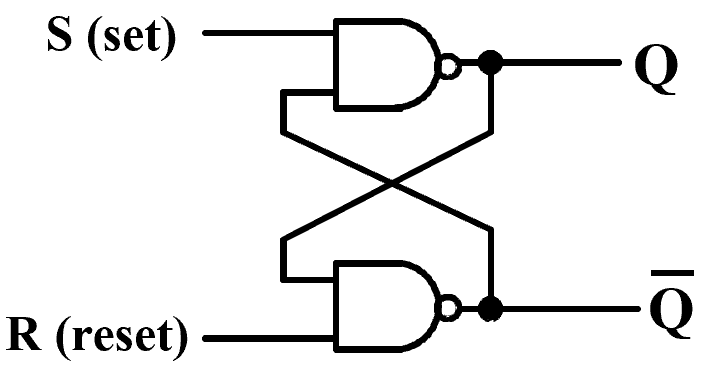
| \(R\) | \(S\) | \(Q\) | \(\overline Q\) | Comment |
|---|---|---|---|---|
| 1 | 1 | ? | ? | Stored state unknown |
| 1 | 0 | 1 | 0 | Set Q to 1 |
| 1 | 1 | 1 | 0 | Now Q remembers 1 |
| 0 | 1 | 0 | 1 | Reset Q to 0 |
| 1 | 1 | 0 | 1 | Now Q remembers 0 |
| 0 | 0 | 1 | 1 | Both go high |
| 1 | 1 | ? | ? | Unstable! |
最后一步,两个引脚同时从 0 -> 1, 那么两个与非门的输出都期望变成 0, 但只要有一个门的输出变为 0 另一个门就被锁住变成 1, 因此两个门不可能同时变化。但我们无法确定是哪个门会变成 1.
\(S=0,R=0\) is forbidden as input pattern.
Basic (NOR) \(S\) – \(R\) Latch
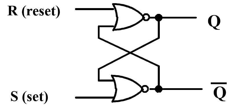
| \(R\) | \(S\) | \(Q\) | \(\overline Q\) | Comment |
|---|---|---|---|---|
| 0 | 0 | ? | ? | Stored state unknown |
| 0 | 1 | 1 | 0 | Set Q to 1 |
| 0 | 0 | 1 | 0 | Now Q remembers 1 |
| 1 | 0 | 0 | 1 | Reset Q to 0 |
| 0 | 0 | 0 | 1 | Now Q remembers 0 |
| 1 | 1 | 1 | 1 | Both go high |
| 0 | 0 | ? | ? | Unstable! |
Clocked \(S\) - \(R\) Latch
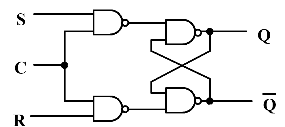
\(C\) 作为一个 ENABLE 的功能。当 \(C=0\) 时,\(Q\) 不会发生改变。当 \(C=1\) 时,上面相当于 \(\overline S\), 下面相当于 \(\overline R\), 变成一个钟控的 SR 锁存器。
| \(C\) | \(S\) | \(R\) | \(Q(t+1)\) |
|---|---|---|---|
| 0 | X | X | No change |
| 1 | 0 | 0 | No change |
| 1 | 0 | 1 | 0: Clear Q |
| 1 | 1 | 0 | 1: Set Q |
| 1 | 1 | 1 | Indeterminate |
\(Q(t+1)\) based on current state \(Q(t)\) and current inputs \((S,R,C)\)
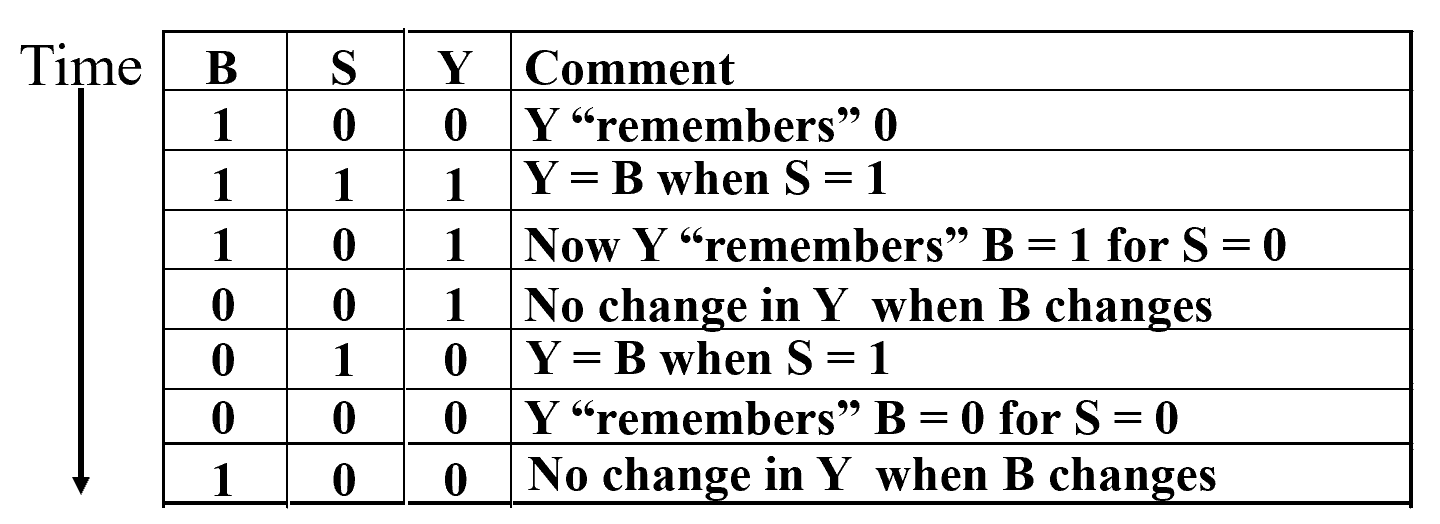
\(D\) Latch
\(S\ R\) 不会同时为 0.
| \(C\) | \(D\) | \(Q(t+1)\) |
|---|---|---|
| 0 | X | No change |
| 1 | 0 | 0: Clear Q |
| 0 | 1 | 1: Set Q |
即当 \(C=1\) 时 \(Q=D\)
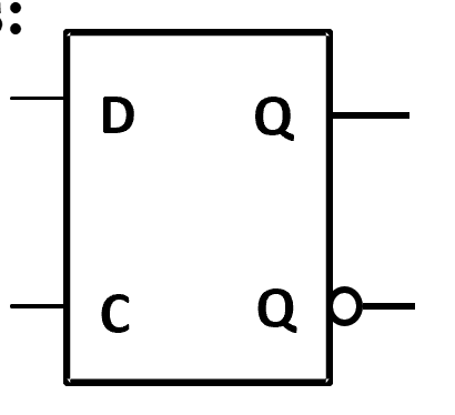
The graphic symbol for a \(D\) latch:
Info
在算门输入成本的时候,我们要分开算 G 和 GN. 因为锁存器同时为我们提供了 \(Q\) 和 \(\overline Q\), 锁存器可以为后面的组合电路提供原变量和反变量。
Flip-flop
锁存器不适合使用在电路中:不能做到一个周期,状态只更新一次。具体原因见 ICS Notes
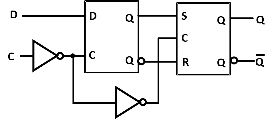
S-R Master-Slave Flip-Flop
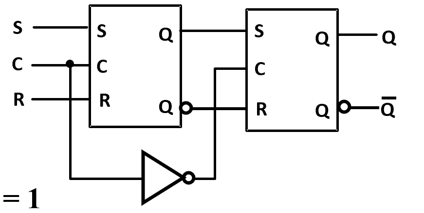
前面称为 master( 主锁存器 ), 后面称为 slave( 从锁存器 )
当 \(C=0\) 时,主锁存器不变。
\(C\) 从 0 变为 1 时,主锁存器被使能,Q 改变,但从锁存器不变。
周期变长一倍
一次性采样问题(1s catching):当 S R 均为 0 时如果有小扰动,无法复原
要求主从触发器避免 S R 的扰动
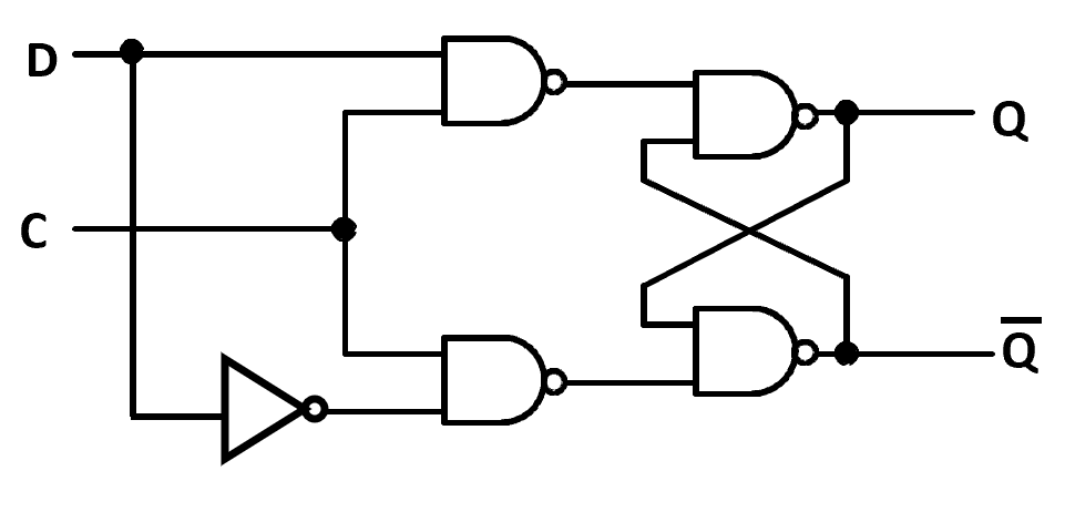
Edge-Triggered D Flip-Flop
An edge-triggered flip-flop ignores the pulse while it is at a constant level and triggers only during a transition of the clock signal.
A master-slave D flip-flop which also exhibits edge-triggered behavior can be used.
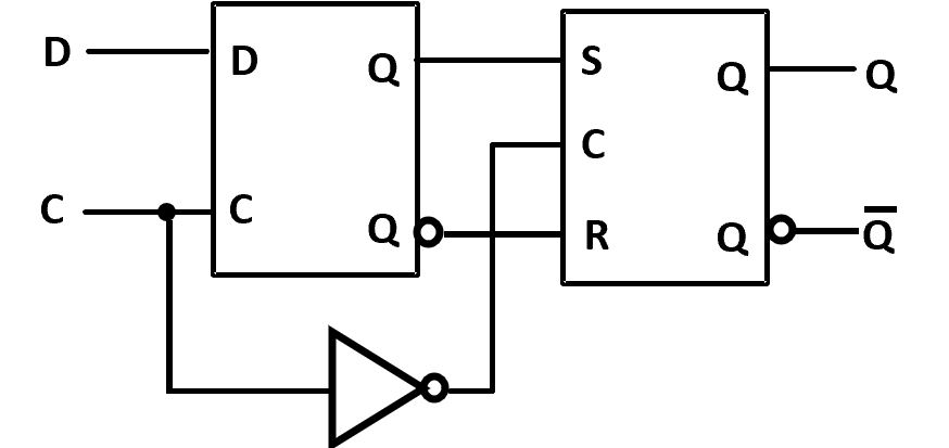
The delay of the S-R master-slave flip-flop can be avoided since the 1s-catching behavior is not present with D replacing S and R inputs. (D 锁存器不会出现 S R 同时为 0 的情况 )
Positive-Edge Triggered D Flip-Flop is Formed by adding inverter to clock input. ( 上升沿触发器 )
Q changes to the value on D applied at the positive clock edge within timing constraints to be specified
Actual Circuit of Edge-Triggered D Flip-Flop:

( 和 D-Latch Flip-flop 有所不同 )
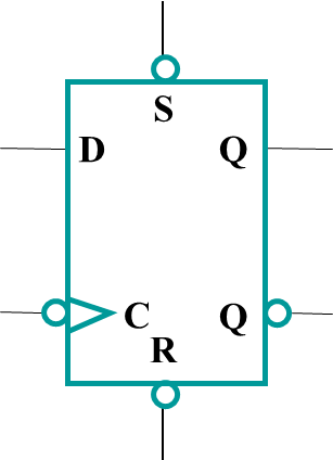
Standard Symbols for Storage Elements:
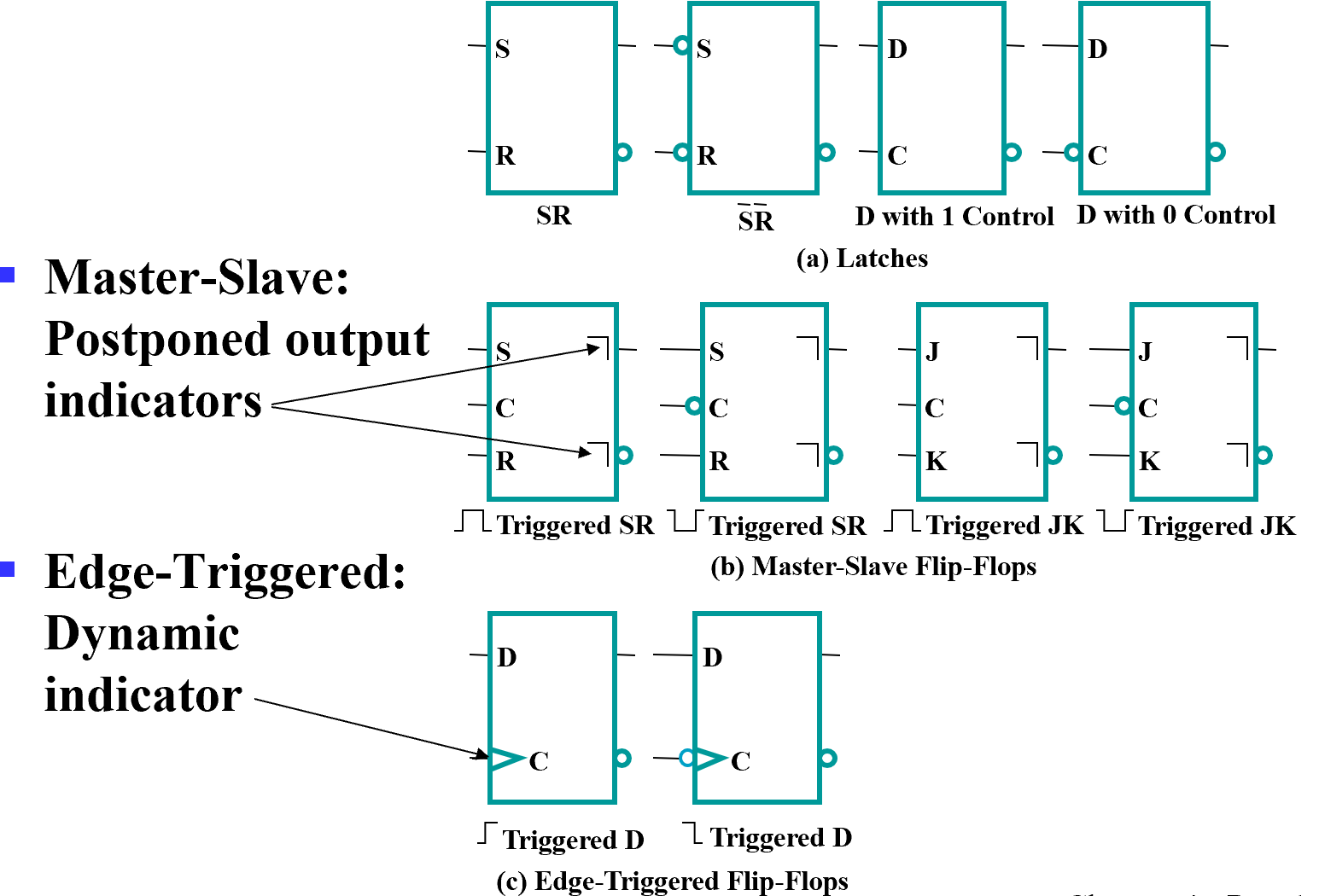
- Direct Inputs
Direct \(R\) and/or \(S\) inputs that control the state of the latches within the flip-flops are used for this initialization.
Analysis
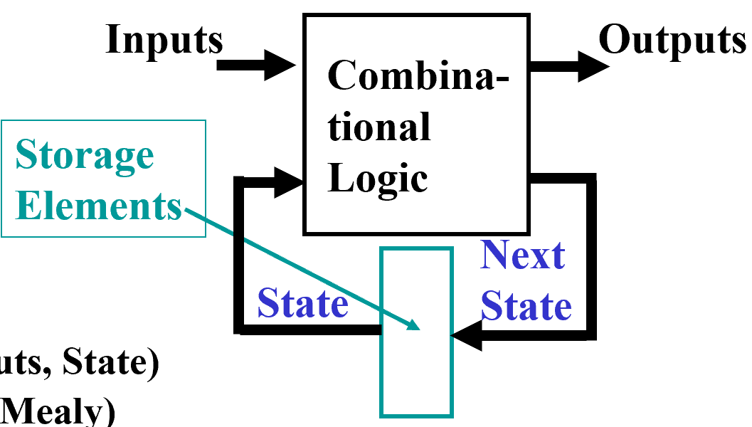
General Model
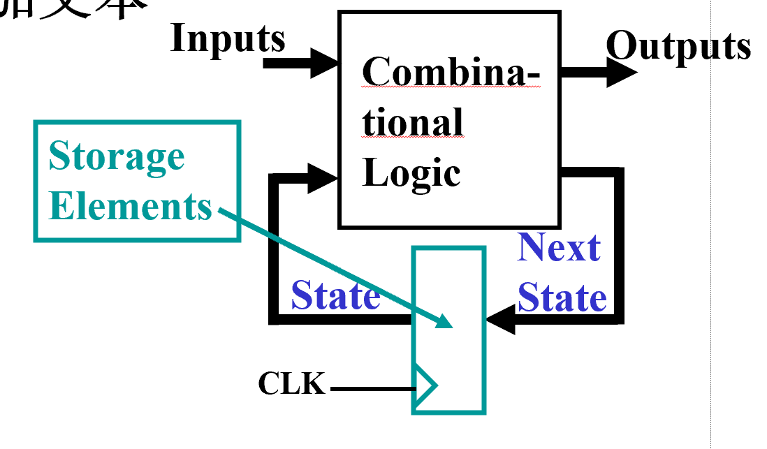
同步时序电路里 D 触发器的时钟输入端,统一接在一个系统时钟输入 CLK 信号上
- Current State at time (t) is stored in an array of flip-flops.
- Next State at time (t+1) is a Boolean function of State and Inputs.
- Outputs at time (t) are a Boolean function of State (t) and (sometimes) Inputs (t).
Example
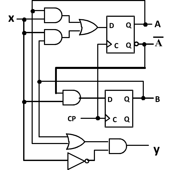
可以看到,cp 是时钟输入信号
- input: \(x(t)\)
- output: \(y(t)\)
-
state: \((A(t),B(t))\)
-
Boolean equations for the functions \(D_A(t) = A(t)x(t)+ B(t)x(t), A(t+1)=A(t)x(t)+ B(t)x(t)\),
\(D_B(t) = A(t)x(t),B(t+1) = A(t)x(t), y(t) = x(t)(B(t) + A(t))\)
State table
- Present State – the values of the state variables for each allowed state.
- Input – the input combinations allowed.
- Next-state – the value of the state at time \((t+1)\) based on the present state and the input.
- Output – the value of the output as a function of the present state and (sometimes) the input.
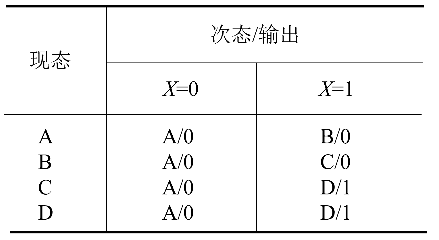
Example
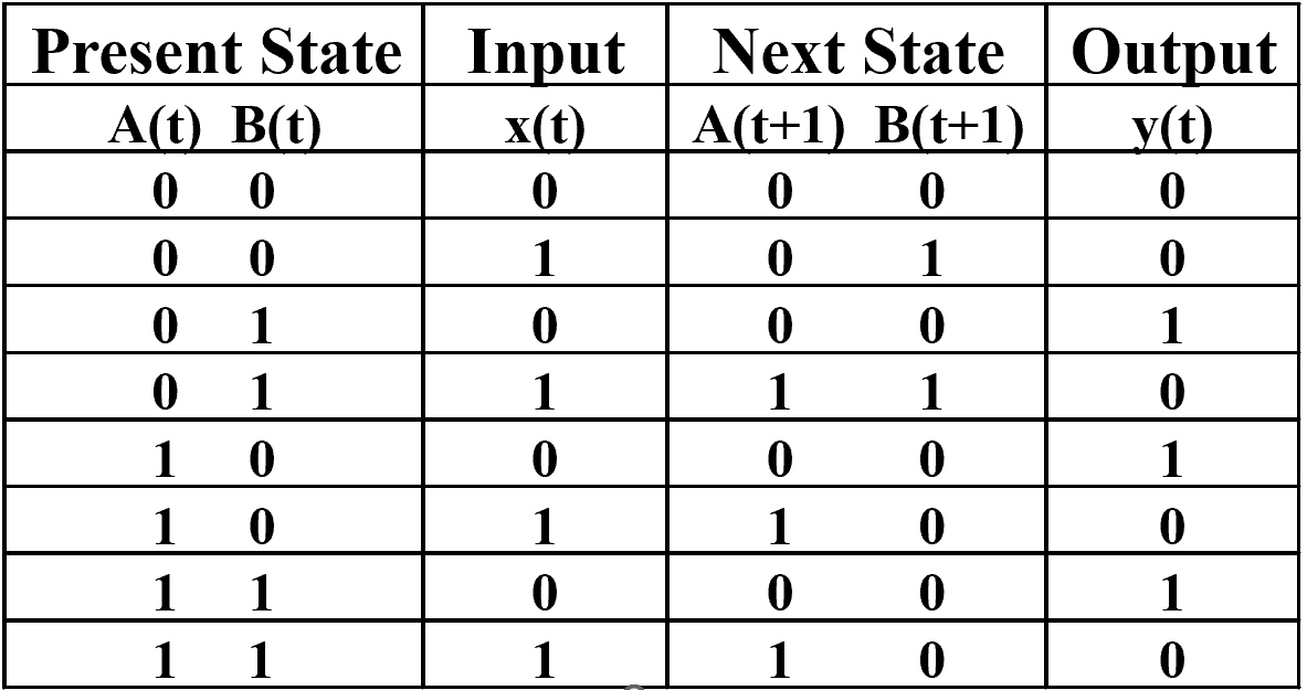
代入刚刚写出的式子即可
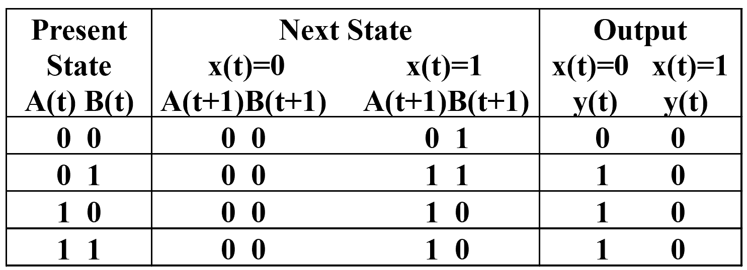
也可以使用另一种画法:(二维状态表,按照格雷码的顺序排列)
Note
在画状态表时,无法达到的状态也要画出来。因为可能程序受到某种扰动或者异常,可能会跳到原先无法到达的状态。
State Diagrams
The sequential circuit function can be represented in graphical form as a state diagram with the following components:
- A circle with the state name in it for each state
- A directed arc from the Present State to the Next State for each state transition
- A label on each directed arc with the Input values which causes the state transition, and A label:
输出和输入是否有关,无关标在圈里面,有关标在外面- On each circle with the output value produced, or
- On each directed arc with the output value produced.
Moore type output depends only on state( 输出画在圈里面 )
Mealy type output depends on state and input( 输出画在有向弧上 )
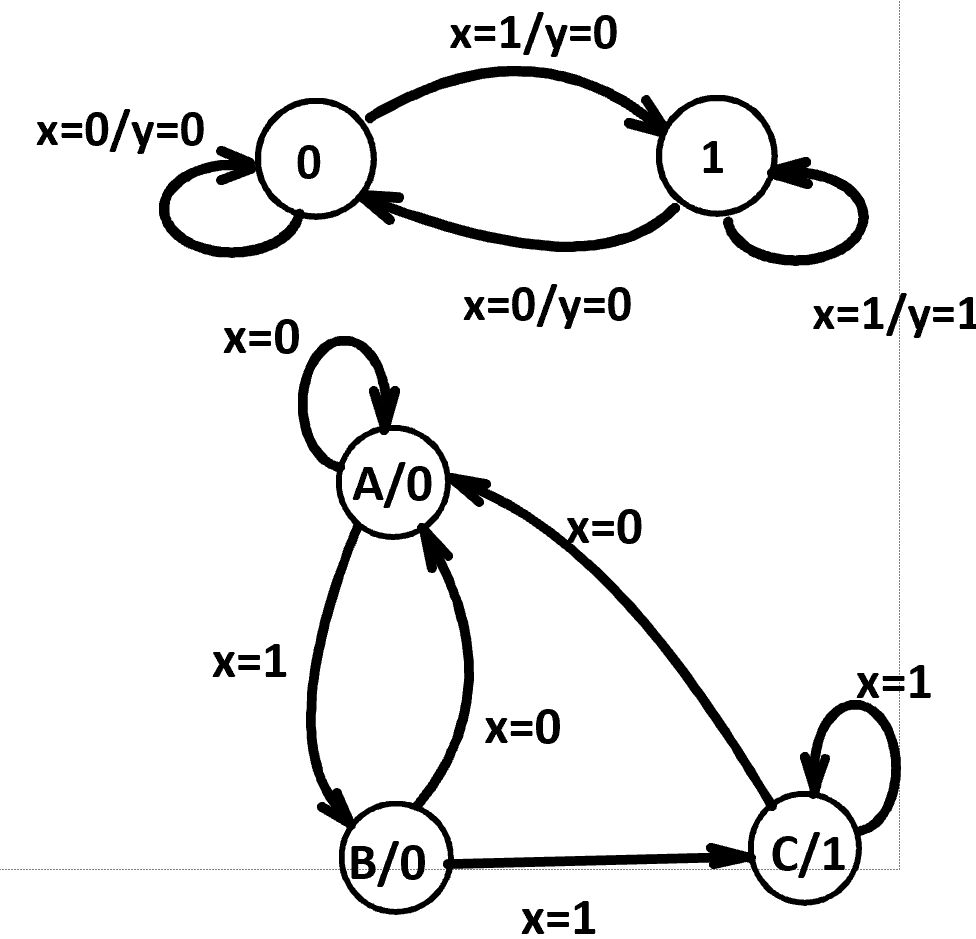
Example

(斜杠左边表示外部输入,右边表示输出)
Sequential Circuits or Sequential Machines are also called Finite State Machines (FSMs).
-
Equivalent State Definitions
两个状态,无论输入是什么,都会使这两个状态输出相同,次态也相同,那么这两个状态是等效状态。Example

在这个图里我们可以发现 S2, S3 是等效状态。
合并 S2, S3 后:
这个时候我们发现 S1 和 S2 又是等效状态,再次合并,最后得到:

为什么要合并等效状态
减少表示状态所需要的二进制位
Moore and Mealy Example Diagrams
Flip-Flop Timing Parameters
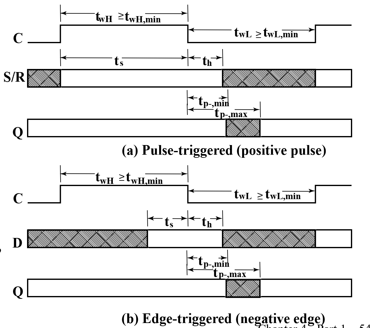
- \(t_s\) - setup time. 在下降之前要先准备好。
- \(t_h\) - hold time
- \(t_w\) - clock pulse width
- \(t_{px}\) - propagation delay. Measured from clock edge that triggers the output change to the output change.
主从触发器和边缘触发器的 \(t_s\)
根据定义 , \(t_s\) 指在采样前触发器需要的准备时间。对于主从触发器,在信号处于上升沿的时候 S 部分的输入是不能改变的,否则可能有一次性采样问题,因此在信号处于上升沿都是触发器的准备时间。这也是为什么现在我们普遍使用边缘触发器的原因。
对于 D 触发器而言,不要卡在时钟边沿改变 D 的输入,而是在时钟改变之前就进行,这样 D 触发器才能有足够的准备时间。
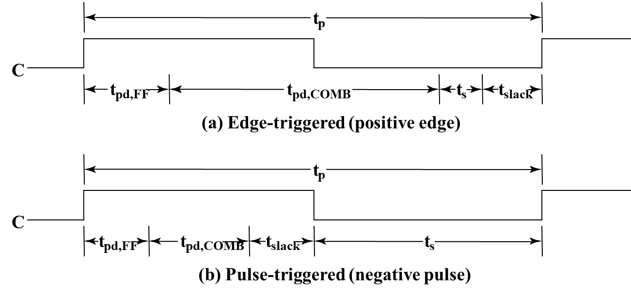
- \(t_p\) - clock period
- \(t_{pd,COMB}\) - total delay of combinational logic along the path from flip-flop output to flip-flop input
- \(t_{slack}\) - extra time in the clock period in addition to the sum of the delays and setup time on a path. 松弛时间(休息)必须大于等于 0.
Time equation: \(t_p \geq \max (t_{pd,FF} + t_{pd,COMB} + t_s)\) for all paths from flip-flop output to flip-flop input.
Example
Compare the allowable combinational delay for a specific circuit: Using edge-triggered flip-flops; Using master-slave flip-flops.
- Parameters: clock frequency = 250 Mhz; \(t_{pd,FF}(max)=1.0ns\); \(t_s(max)=0.3ns\) for edge-triggered flip-flops; \(t_s = t_{wH} = 2.0 ns\) for master-slave flip-flops
- Calculation: \(t_p = \dfrac{1}{clock\ frequency} = 4.0 ns\)
- Edge-triggered: \(4.0 \geq 1.0 + t_{pd,COMB} + 0.3, t_{pd,COMB} \leq 2.7 ns\)
- Master-slave: \(4.0 \geq 1.0 + t_{pd,COMB} + 2.0, t_{pd,COMB} \leq 1.0 ns\)
Sequential Circuit Design
The Design procedure
- Specification 需求和功能的描述,一般以文字形式
- Formulation - Obtain a state diagram or state table
- State Assignment - Assign binary codes to the states
- Flip-Flop Input Equation Determination - Select flip-flop types and derive flip-flop equations from next state entries in the table
- Output Equation Determination - Derive output equations from output entries in the table
- Optimization - Optimize the equations
- Technology Mapping - Find circuit from equations and map to flip-flops and gate technology
- Verification - Verify correctness of final design
Formulation
A state is an abstraction of the history of the past applied inputs to the circuit (including power-up reset or system reset).
将文本化的需求变为用状态机描述(整个电路经过哪些状态?每个状态之间由哪个输入进行驱动?输出是什么
这里我们以 Sequence Recognizers 为例,介绍 Formulation 的过程。
Sequence Recognizers
A sequence recognizer is a sequential circuit that produces a distinct output value whenever a prescribed pattern of input symbols occur in sequence, i.e, recognizes an input sequence occurence.
To develop a sequence recognizer state diagram:
- Begin in an initial state in which NONE of the initial portion of the sequence has occurred (typically “reset” state).
- Add a state that recognizes that the first symbol has occurred.
- Add states that recognize each successive symbol occurring.
- The final state represents the input sequence (possibly less the final input value) occurence.
- Add state transition arcs which specify what happens when a symbol not in the proper sequence has occurred.
- Add other arcs on non-sequence inputs which transition to states that represent the input subsequence that has occurred.
Example
这里我们以识别 1101 为例 .(Mealy 模型 )
after 110 and a 1, we have:

注意在 D 状态之后,应该与 B 状态相连 ( 因为 1101101) 中的第三个 1 既可以是前一个序列的末尾 1, 也可以是下一个序列的起始 1.
我们补足状态之间的转移:
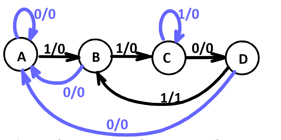
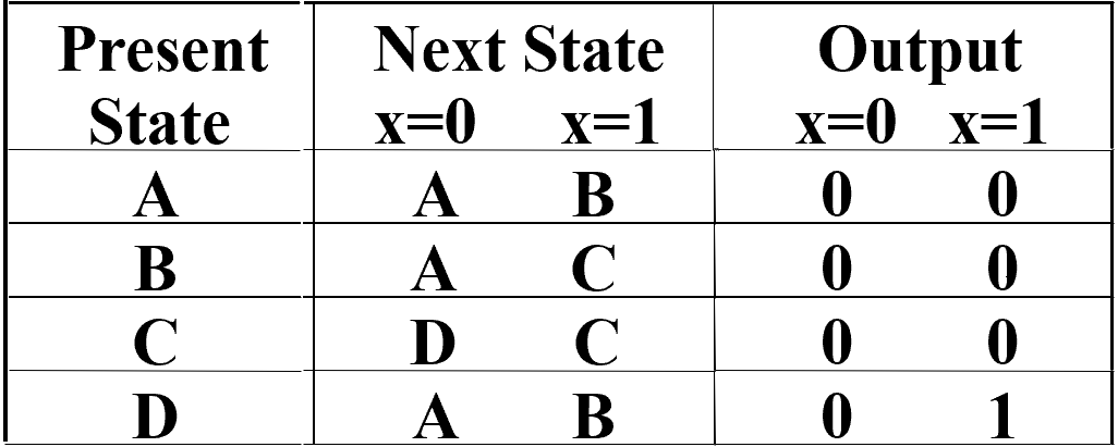
通过状态图得到状态表 :
如果将刚刚的状态图 转为 Moore 模型,我们需要再加一个状态 E, 当到达 E 状态时表明我们得到了序列 1101.
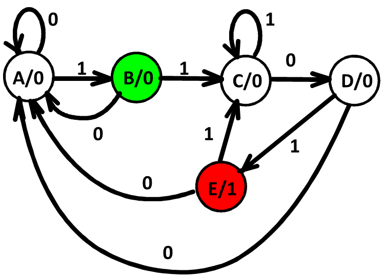
观察可以发现 , B 和 E 对同样的输入,次态都是一样的。但是并不是等效状态,因为二者的输出不同。
The Moore model for a sequence recognizer usually has more states than the Mealy model.
Simplification for State Tables
所谓状态简化,就是要获得一个最小化的状态表。这个表不仅能正确地反映设计的全部要求,而且状态的数目最少。
“状态等效” 的三种情况
- 首先,输出相同
-
同时,次态相同 / 次态交错 / 次态循环
等效
-
次态相同

-
次态相同或交错
-
次态交错或等效

-
次态交错或相同或循环

-
状态简化方法:
-
观察法
Example
- \(A\) 和 \(B\),\(C\) 和 \(D\) 的输出完全相等;
- \(C\) 和 \(D\) 在输入的各种取值组合下,次态相同,因此 \(C\) 和 \(D\) 等效;
- \(A\) 和 \(B\) 在 \(X=1\) 时的次态不满足四条件之一,因此 \(A\) 和 \(B\) 不等效 ;
- 最大等效类为 \(\{A\},\{B\},\{C,D\}\), 分别用 \(A', B', C'\) 表示;
-
隐含表法化简
- 作隐含表
- 顺序比较,寻等效状态对
- 状态对等效,打“√”;
- 状态对不等效,打“×”;
- 状态对是否等效需进一步检查,则标记次态对。
- 进行关连比较,确定等效状态对
- 确定最大等效类,作最小化状态表
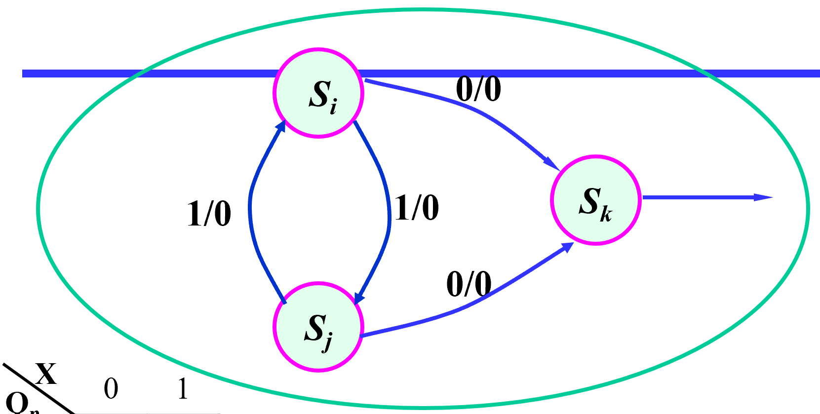
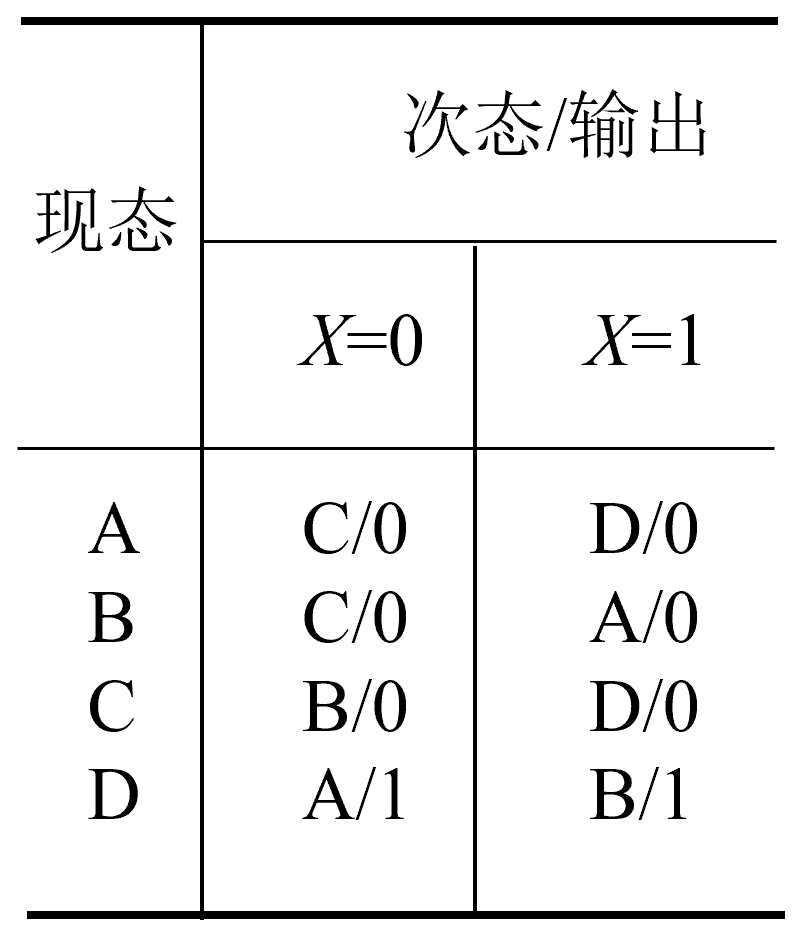
Example


由于 \(CD\)、\(DE\) 不等效,所以 \(DG\) 不等效,画斜线标志。最后我们有 \(AB\rightarrow CF\) \(AE→BE→CF\). 处于循环链中的每一个状态对都是等效状态对。
最后我们有- 四个等效对 \((A,B), (A,E), (B,E), (C,F)\)
- 最大等效类 \((A,B,E)\)
- 四个状态 \((A,B,E), (C,F), (D), (G)\)
- 令以上四个状态依次为 \(a, b, c, d\)
State Assignment
Each of the \(m\) states must be assigned a unique code
Minimum number of bits required is \(n\) such that \(n\geq \lceil \log_2 m\rceil\)
There are \(2^n - m\) unused states. ( 不能省略,可能会因为异常陷入 unused states)
Different State Assignment

-
Counting Order Assignment: \(A = 0 0, B = 0 1, C = 1 0, D = 1 1\)
-
Gray Code Assignment: \(A = 0 0, B = 0 1, C = 1 1, D = 1 0\)
状态分配的方案不一样,所得到的输出函数和激励函数的表达式也不同,由此而设计出来的电路复杂度也不同。状态分配的任务是:
- 决定编码的长度
- 寻找一种最佳(很难找到)的或接近最佳的状态分配方案
分配的基本原则 :
- 在相同输入条件下具有相同次态的现态,应尽可能分配相邻的二进制代码
- 在相邻输入条件,同一现态的次态应尽可能分配相邻的二进制代码
- 输出完全相同的现态应尽可能分配相邻的二进制代码
- 最小化状态表中出现次数最多的状态或初始状态应分配逻辑 0
- 一般情况下,第一条原则较为重要,需优先考虑,其次要考虑由前三条原则得到的应分配相邻代码的状态对出现的次数,次数多的状态对应优先分配相邻的二进制代码。
Example
- 在相同输入条件下具有相同次态的现态,应尽可能分配相邻的二进制代码:A 和 B,A 和 C 应相邻
- 在相邻输入条件,同一现态的次态应尽可能分配相邻的二进制代码:C 和 D,C 和 A,B 和 D,A 和 B 应相邻;
- 输出完全相同的现态应尽可能分配相邻的二进制代码: A,B,C 三者应相邻,即 A 和 B,A 和 C,B 和 C 应相邻;
- 最小化状态表中出现次数最多的状态或初始状态应分配逻辑 0:A 分配为逻辑 0
最后得到 :

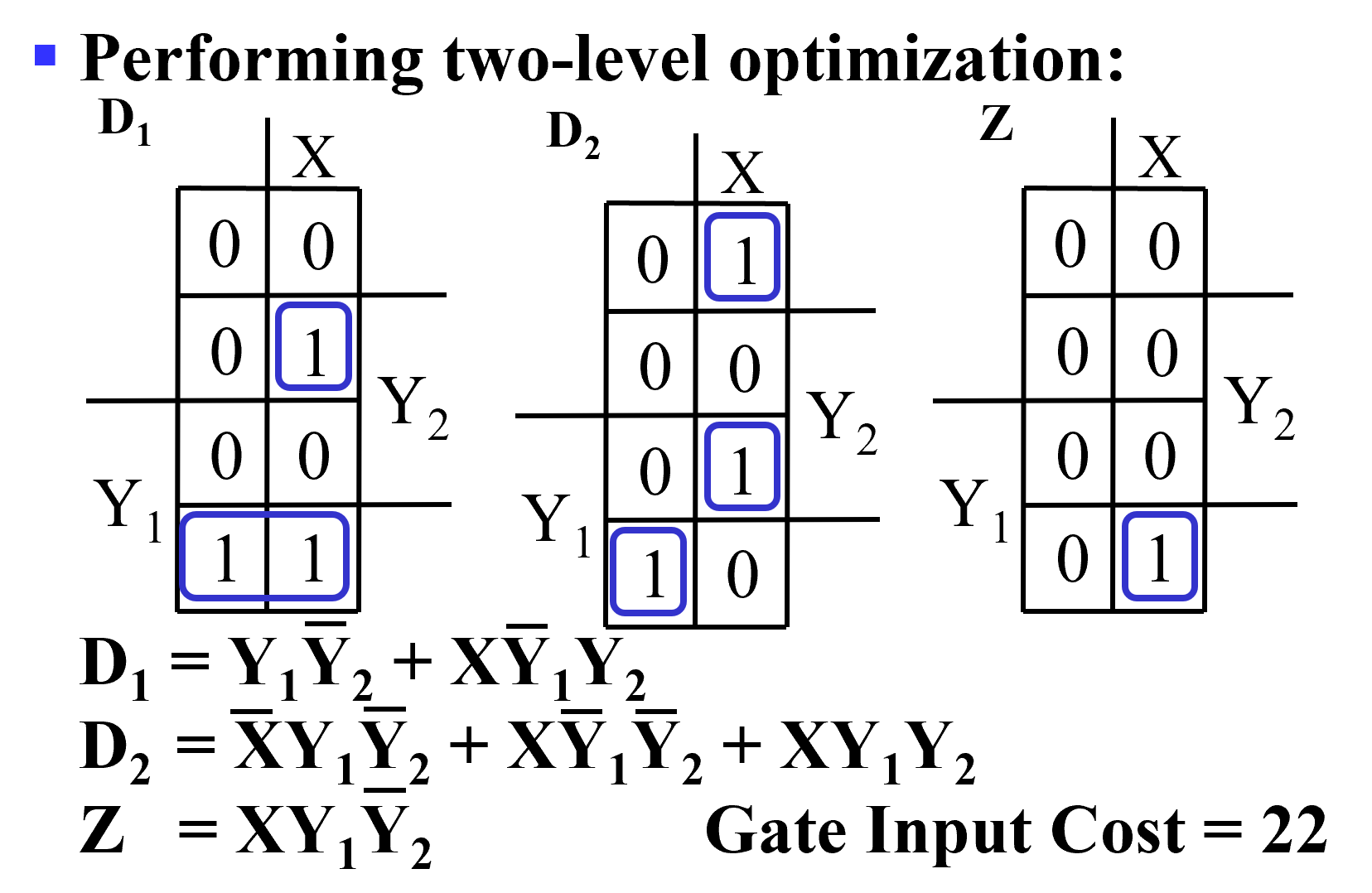
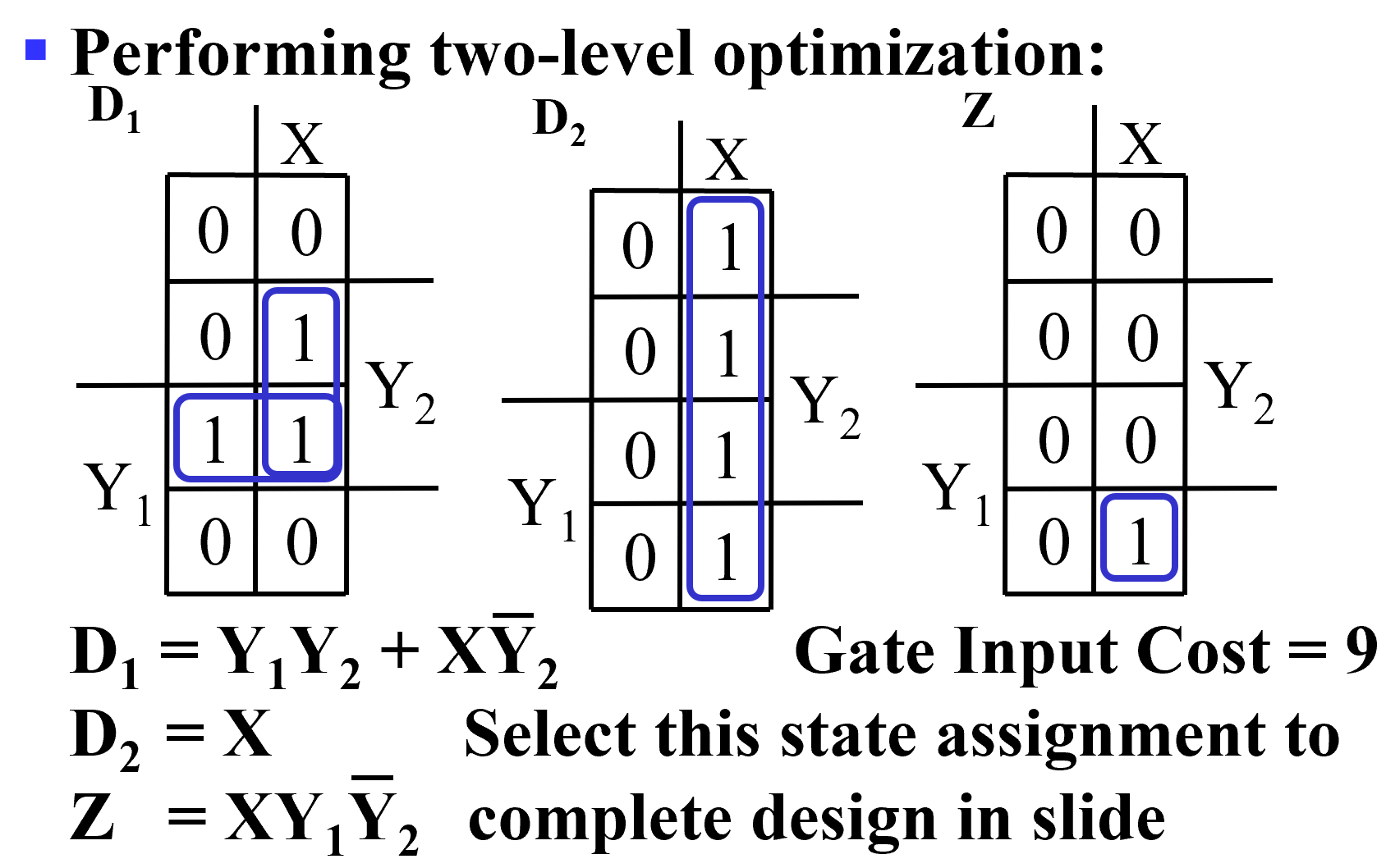
Technology Mapping
Library: D flip-flops with Reset(not inverted), NAND gates with up to 4 inputs and inverters.
方法同之前,先将与门或门等门转化为 NAND, 随后将 inverter 推出散出点。
Other Flip-Flop Types
J-K Flip-flop
- Behavior
- 类似 SR 触发器 , \(J\) 相当于 \(S\), \(K\) 相当于 \(R\).
- 但 \(J=K=1\) 时,触发器相当于是一个求反的功能
- 也有一次性采样的问题
-
Implementation

-
Symbol
 (三角表明是上升沿触发,若为圆圈则是下降沿触发)
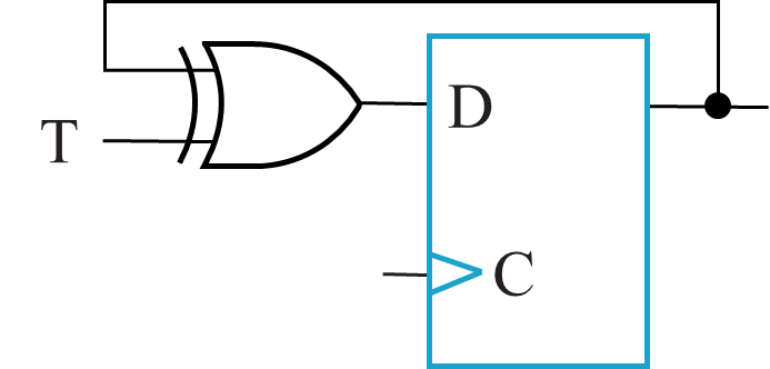
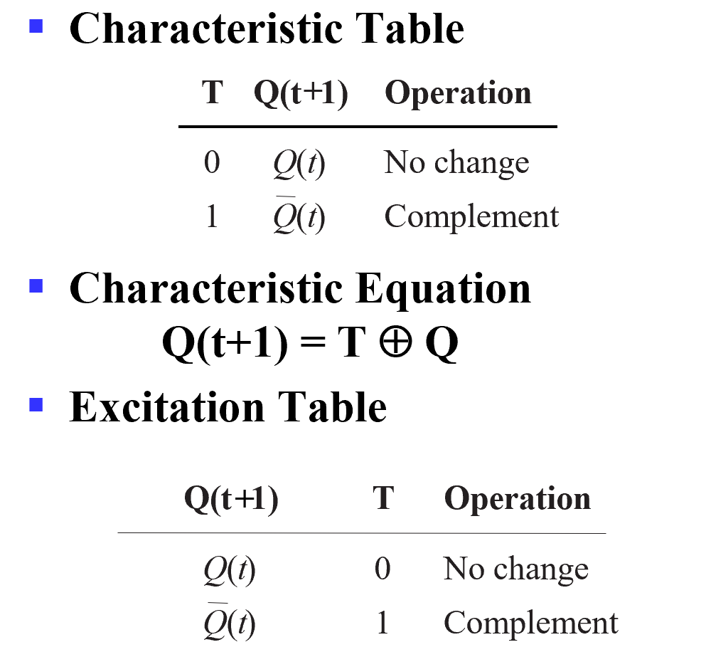
T Flip-flop
- Behavior
- 类似 JK 触发器 , 相当于 \(J=K=T\). 当 \(T = 0\), 状态不变 ; 当 \(T = 1\), 状态求反
- 存在一次性采样的问题
- 无法预置状态,因此需要一个 Reset 信号
-
Implementation
-
Symbol

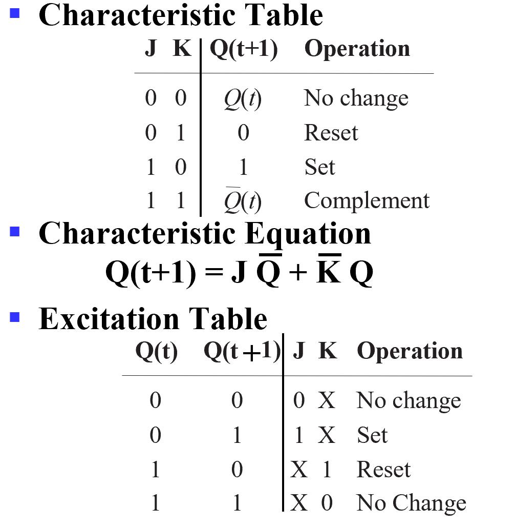
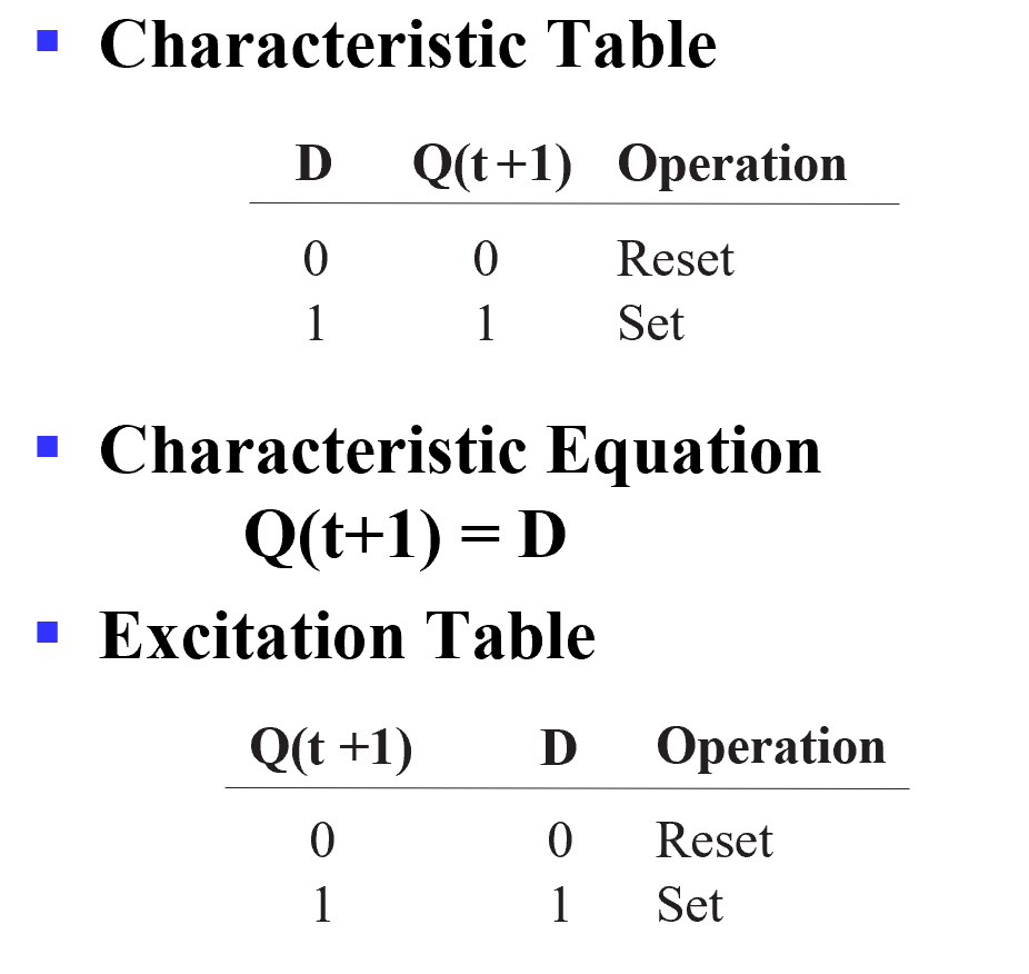
Basic Flip-Flop Descriptors
- Used in analysis
已知触发器的输入和现态,预测触发器的输出和次态- Characteristic table - defines the next state of the flip-flop in terms of flip-flop inputs and current state
- Characteristic equation - defines the next state of the flip-flop as a Boolean function of the flip-flop inputs and the current state
- Used in design
已知现态和次态,预测我们要提供怎样的输入- Excitation table( 激励表 ) - defines the flip-flop input variable values as function of the current state and next state
D Flip-Flop Descriptors
T Flip-Flop Descriptors
S-R Flip-Flop Descriptors
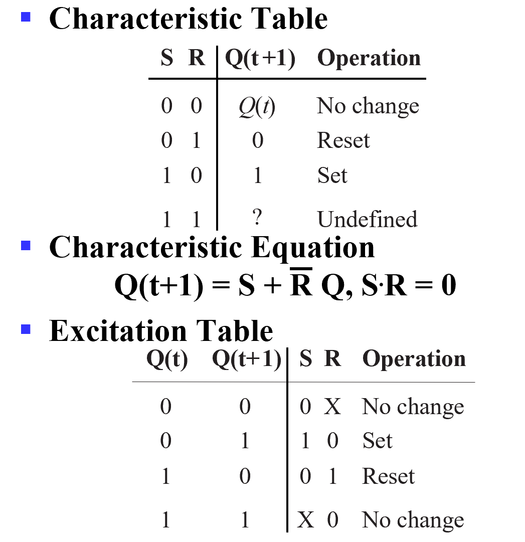 ( 注意这里有个条件 S R 不能同时为 1.)
 J-K Flip-Flop Descriptors